A blank ceramic substrate is an unmetallized, as-fired or as-lapped ceramic plate used as the starting material for printed-circuit metallization, thin-film deposition, direct bonded copper (DBC), active metal brazing (AMB), or die-attach processes. It carries no conductors, no vias, and no surface finish—just the ceramic body itself, ready for downstream processing. Choosing the right blank determines everything that follows: adhesion strength, line resolution, thermal resistance, and long-term reliability.
This page covers the materials, grades, dimensional specs, surface conditions, and selection logic you need to specify blank ceramic substrates for your project.
Key Takeaways
- The four most common blank ceramic substrate materials are 96% Al₂O₃, 99.6% Al₂O₃, aluminum nitride (AlN), and silicon nitride (Si₃N₄), each suited to different thermal, mechanical, and electrical requirements.
- As-fired alumina substrates typically have a surface roughness (Ra) of 0.4–0.8 µm; lapped and polished surfaces can reach Ra ≤ 0.05 µm, which matters for thin-film metallization yield.
- Thermal conductivity spans a wide range: 24–28 W/m·K for 96% alumina, 35–36 W/m·K for 99.6% alumina, 170–200 W/m·K for AlN, and 70–90 W/m·K for Si₃N₄.
- Blank substrates are available in standard panel sizes (typically 2″×2″ up to 4.5″×4.5″ or larger) and thicknesses from 0.25 mm to 2.0 mm, with custom-shape ceramic substrates laser-scribed or machined to order.
- The downstream metallization process—thick film, thin film, DPC, DBC, or AMB—dictates minimum surface quality, camber, and flatness requirements for the blank.
What Is a Blank (As-Fired) Ceramic Substrate?
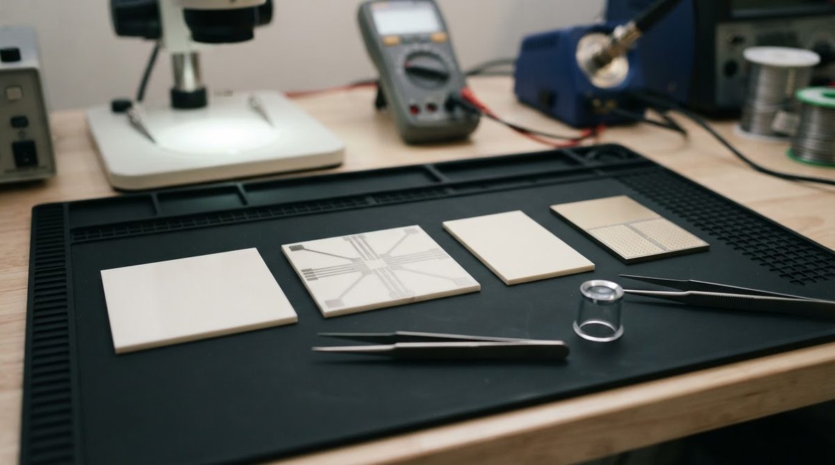
A blank ceramic substrate is the base plate before any metal, paste, or circuit pattern is applied. The term “as-fired” refers to the condition of the ceramic after sintering in a kiln—the final densification step that converts a green (unfired) ceramic body into a hard, dense part. Some blanks receive additional post-fire processing such as lapping, polishing, or laser scribing, but they are still considered “blank” as long as no metallization has been applied.
Blank substrates serve as the foundation for multiple downstream processes. A thick-film house screen-prints conductor pastes onto the blank. A thin-film facility sputters or evaporates metal layers. A DBC manufacturer bonds a copper foil at high temperature directly to the oxide surface. In each case, the blank’s material purity, surface roughness, flatness, and dimensional tolerance directly affect circuit quality and yield.
If you need substrates that already carry copper, silver, or gold conductors, see metallized ceramic substrates instead. This page focuses strictly on the unmetallized starting material.
Material Grades for Blank Ceramic Substrates
Four ceramic materials account for the vast majority of blank substrates used in electronics. Each has a distinct combination of thermal conductivity, dielectric strength, mechanical toughness, and cost. The right choice depends on your operating environment, the metallization process you will use, and your budget.
96% Alumina (Al₂O₃ 96%)
This is the workhorse. Roughly 70–80% of all ceramic substrates shipped globally are 96% alumina. The “96%” refers to the alumina content by weight; the remaining 4% is a glass-phase binder (typically SiO₂, MgO, and CaO) that lowers the sintering temperature and improves manufacturability. The glass phase also slightly reduces thermal conductivity compared to higher-purity grades.
96% alumina blanks are compatible with virtually every metallization method: thick film, thin film, DPC, DBC, and AMB. They are the default substrate for hybrid microelectronics, power LED submounts, sensor packages, and general-purpose ceramic PCBs. Detailed product specs for various processing routes are available on the 96% alumina thick-film substrate, 96% alumina thin-film substrate, 96% alumina DPC substrate, 96% alumina DBC substrate, and 96% alumina AMB substrate pages.
Typical cost for a 96% alumina blank in standard sizes runs $0.50–$3.00 per piece at volume, depending on dimensions and surface finish. This is the lowest-cost ceramic substrate option by a wide margin.
99.6% Alumina (Al₂O₃ 99.6%)
Increasing alumina purity to 99.6% eliminates most of the glass-phase binder. The result is higher thermal conductivity (35–36 W/m·K vs. 24–28 W/m·K for 96%), better high-frequency dielectric performance, and improved chemical resistance. The trade-off is a higher sintering temperature (~1,700 °C vs. ~1,600 °C for 96%), which increases manufacturing cost by roughly 30–60%.
99.6% alumina blanks are preferred for thin-film circuits requiring tight line resolution (≤25 µm trace/space), high-frequency RF substrates, and applications where operating temperatures exceed 300 °C for extended periods. The lower glass content reduces dielectric loss at microwave frequencies, making this grade a better choice for millimeter-wave circuits than 96% alumina.
For downstream metallization options, see 99.6% alumina thick-film substrate, 99.6% alumina thin-film substrate, and 99.6% alumina DPC substrate.
Aluminum Nitride (AlN)
AlN substrates offer thermal conductivity of 170–200 W/m·K—roughly 6–8× that of 96% alumina—while maintaining excellent electrical insulation (dielectric strength >15 kV/mm). This makes AlN the material of choice for high-power electronics: IGBT modules, SiC and GaN power devices, high-brightness LED arrays, and laser diode submounts where junction temperature must be minimized.
AlN is more expensive than alumina (typically 5–10× per unit area at equivalent dimensions) and more difficult to machine. It also requires careful handling: AlN is sensitive to moisture in its green state, and fired AlN can degrade in humid environments above 80 °C unless a protective surface treatment is applied. Most AlN blanks intended for metallization are supplied with an oxidized surface layer that improves wettability for brazing and bonding.
AlN blanks are available for AlN thick-film processing and AlN thin-film processing. For substrates already carrying copper metallization, see copper-metallized aluminum nitride substrates. To purchase AlN blanks directly, visit the buy aluminum nitride substrate page.
Silicon Nitride (Si₃N₄)
Si₃N₄ substrates combine moderate thermal conductivity (70–90 W/m·K) with exceptional mechanical strength. Flexural strength ranges from 600–900 MPa per ASTM C1161, compared to 300–380 MPa for 96% alumina and 300–350 MPa for AlN. Fracture toughness (KIC) is 6–7 MPa·m½, roughly 2× that of alumina.
This mechanical advantage matters in applications subject to thermal cycling, vibration, or mechanical shock—particularly automotive power modules (traction inverters), railway converters, and wind-turbine power electronics. Si₃N₄ substrates survive thermal-shock cycles that would crack alumina or AlN blanks of the same thickness, allowing designers to use thinner substrates (0.32 mm is common) to reduce thermal resistance without sacrificing reliability.
Si₃N₄ blanks are the most expensive of the four common ceramics, typically 8–15× the cost of 96% alumina. They are primarily used with AMB or DBC metallization. To order Si₃N₄ blanks, see the buy silicon nitride substrate page.
Other Substrate Materials
Beyond the four main ceramics, specialized applications use additional materials:
- Sapphire (single-crystal Al₂O₃): Used for GaN epitaxy, optical windows, and high-frequency substrates where near-zero porosity and optical transparency are required. See sapphire substrates.
- Quartz (fused SiO₂): Extremely low dielectric constant (3.78 at 1 MHz) and loss tangent, making it ideal for RF filters, MEMS resonators, and photonic circuits. See quartz substrates.
- Borosilicate glass: Low cost, good CTE match to silicon (~3.3 ppm/°C), used for MEMS packaging and microfluidic devices. See borosilicate glass substrates.
Each of these has a narrower application range than alumina or AlN. If you are unsure which material fits your project, the comparison table below will help.
Blank Ceramic Substrate Properties: Comparison Table
| Parameter | 96% Al₂O₃ | 99.6% Al₂O₃ | AlN | Si₃N₄ | Unit | Test Standard / Condition |
|---|---|---|---|---|---|---|
| Thermal conductivity | 24–28 | 35–36 | 170–200 | 70–90 | W/m·K | ASTM E1461, at 25 °C |
| Dielectric constant (εr) | 9.4–9.8 | 9.8–10.0 | 8.5–9.0 | 8.0–8.5 | — | 1 MHz, 25 °C |
| Dielectric strength | >10 | >12 | >15 | >12 | kV/mm | ASTM D149 |
| Loss tangent (tan δ) | 1–3 × 10⁻⁴ | 0.5–1 × 10⁻⁴ | 1–5 × 10⁻⁴ | 1–5 × 10⁻⁴ | — | 1 MHz, 25 °C |
| Flexural strength | 300–380 | 350–400 | 300–350 | 600–900 | MPa | ASTM C1161, 3-point bend |
| Fracture toughness (KIC) | 3.5–4.0 | 3.8–4.2 | 2.5–3.5 | 6.0–7.0 | MPa·m½ | ASTM C1421 |
| CTE (20–300 °C) | 7.0–7.4 | 7.2–7.6 | 4.4–4.7 | 2.8–3.2 | ppm/°C | ASTM E228 |
| Volume resistivity | >10¹⁴ | >10¹⁴ | >10¹⁴ | >10¹² | Ω·cm | ASTM D257, 25 °C |
| Density | 3.72–3.78 | 3.89–3.96 | 3.26–3.30 | 3.20–3.28 | g/cm³ | ASTM C373 |
| Max continuous use temp. | ~1,600 | ~1,700 | ~1,000 (in air) | ~1,200 (in air) | °C | Manufacturer recommendation |
| Typical blank cost (relative) | 1× | 1.3–1.6× | 5–10× | 8–15× | — | Relative to 96% Al₂O₃ |
Typical values for commercially available material, for comparison only. Confirm against the datasheet for your specific grade. Data compiled from CoorsTek, Kyocera, and Maruwa published datasheets. For downloadable specs, see the ceramic substrate datasheet library.
Dimensional Specifications: Sizes, Thicknesses, and Tolerances
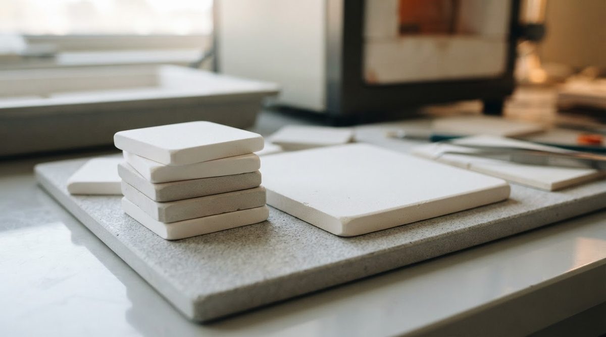
Blank ceramic substrates are manufactured in standard panel sizes and then either shipped as-is or scribed/diced into smaller pieces. Understanding available sizes and tolerances helps you avoid unnecessary custom tooling charges and long lead times.
Standard Panel Sizes
The most common standard sizes for blank alumina substrates are:
- 1″ × 1″ (25.4 × 25.4 mm)
- 2″ × 2″ (50.8 × 50.8 mm)
- 3″ × 3″ (76.2 × 76.2 mm)
- 4.5″ × 4.5″ (114.3 × 114.3 mm)
- Some suppliers offer up to 190 × 190 mm panels for alumina
AlN and Si₃N₄ blanks are typically available in smaller maximum sizes due to sintering constraints—commonly up to 114.3 × 114.3 mm for AlN and 190 × 140 mm for Si₃N₄, though this varies by manufacturer. A full listing of stock dimensions is on the standard ceramic substrate sizes page.
Thickness Options
Standard blank substrate thicknesses range from 0.25 mm to 2.0 mm. The most commonly specified values are:
| Thickness (mm) | Typical Application | Notes |
|---|---|---|
| 0.25 | Thin-film circuits, LED submounts | Fragile; handle with care. Requires vacuum chucks for processing. |
| 0.32 | Si₃N₄ power modules, DBC | Common for automotive traction inverters (Si₃N₄ only). |
| 0.38 | DBC substrates, general thin-film | Widely stocked in alumina and AlN. |
| 0.50 | Thick-film hybrid circuits | Good balance of strength and thermal resistance. |
| 0.635 | Standard thick-film substrates | The “classic” 25-mil substrate. Most widely stocked dimension. |
| 1.0 | High-voltage insulation, structural | Higher dielectric withstand; heavier. |
| 1.5–2.0 | Heatsink substrates, spacers | Used as structural or thermal-spreading elements. |
For a visual guide to all available gauges, refer to the ceramic substrate thickness chart.
Dimensional and Flatness Tolerances
Tolerances for as-fired blanks depend on the material, the firing method, and whether post-fire machining (lapping, grinding) is applied.
| Parameter | As-Fired (typical) | Lapped / Ground | Unit |
|---|---|---|---|
| Length / width tolerance | ±0.5–1.0% | ±0.05–0.10 mm | mm |
| Thickness tolerance | ±0.05–0.10 | ±0.01–0.025 | mm |
| Camber (bow) | ≤0.10 mm per 25 mm | ≤0.05 mm per 25 mm | mm/25 mm |
| Surface roughness (Ra) | 0.4–0.8 | 0.05–0.25 | µm |
Values are representative of 96% alumina. AlN and Si₃N₄ may have wider as-fired tolerances due to higher shrinkage variability. Confirm against your supplier’s datasheet.
Camber is particularly important for DBC and AMB processes, where the copper foil must bond uniformly across the entire substrate surface. Excessive camber causes voids, which become stress concentrators during thermal cycling. Most DBC-grade blanks are specified to ≤0.05 mm per 25 mm of length, which typically requires lapping.
Surface Conditions: As-Fired vs. Lapped vs. Polished
The surface condition of a blank ceramic substrate is one of the most critical specifications, because it directly determines which metallization processes will succeed and at what yield.
As-Fired
The as-fired surface is the natural surface left after sintering. For 96% alumina, this is typically Ra 0.4–0.8 µm, with a slightly glassy appearance due to the glass-phase binder migrating to the surface during firing. As-fired surfaces are adequate for thick-film screen printing (conductor, resistor, and dielectric pastes), DBC bonding, and many die-attach applications.
The as-fired surface has micro-porosity and grain pull-out features that actually improve thick-film paste adhesion by providing mechanical interlocking. A surface that is too smooth can reduce thick-film adhesion.
Lapped (Ground)
Lapping removes the top 10–50 µm of the as-fired surface using abrasive slurry on a flat plate. This achieves Ra 0.15–0.30 µm and significantly improves flatness and thickness uniformity. Lapped surfaces are the standard for DPC (direct plated copper) processes and for thick-film applications requiring tight print registration (e.g., multi-layer thick-film circuits with ≤100 µm line/space).
Polished
Polishing takes the surface to Ra ≤ 0.05 µm (sometimes ≤ 0.025 µm for thin-film applications). This mirror-like finish is essential for thin-film metallization via sputtering or evaporation, where any surface defect larger than the film thickness (typically 0.1–2 µm) causes pinholes, opens, or poor adhesion.
Polishing adds significant cost—typically 40–100% over the as-fired blank price—and is only justified when the downstream process demands it. If you are doing thick-film processing, do not specify a polished surface; you will pay more and may get worse paste adhesion.
Surface Condition Selection Guide
| Downstream Process | Recommended Surface | Ra Target (µm) | Why |
|---|---|---|---|
| Thick-film screen print | As-fired or lapped | 0.3–0.8 | Micro-roughness aids paste adhesion |
| Thin-film sputter/evaporate | Polished | ≤0.05 | Prevents pinholes in sub-micron films |
| DPC (direct plated copper) | Lapped | 0.15–0.30 | Seed layer adhesion needs controlled roughness |
| DBC (direct bonded copper) | As-fired or lapped | 0.3–0.8 | Eutectic bonding tolerates moderate roughness |
| AMB (active metal brazing) | Lapped | 0.15–0.40 | Braze filler wetting improves on smoother surfaces |
| Die attach (epoxy or solder) | As-fired | 0.4–0.8 | Roughness aids adhesion; cost-effective |
How Blank Ceramic Substrates Are Manufactured
Understanding the manufacturing process helps you interpret tolerances and specify blanks correctly. The process differs slightly by material, but the general sequence is the same.
Step 1: Powder Preparation
High-purity ceramic powder (Al₂O₃, AlN, or Si₃N₄) is mixed with sintering aids, binders, and plasticizers. For alumina, sintering aids include MgO (to inhibit grain growth), SiO₂, and CaO. For AlN, yttria (Y₂O₃) is the primary sintering aid, promoting densification and forming a grain-boundary phase that influences thermal conductivity.
Step 2: Forming
The powder mixture is formed into “green” (unfired) sheets using one of two methods:
- Tape casting: A slurry is cast onto a moving carrier film using a doctor blade, then dried to form a flexible green tape 0.1–1.0 mm thick. This is the dominant method for thin substrates (≤1.0 mm).
- Dry pressing: Powder is compacted in a die under high pressure (50–200 MPa). Used for thicker substrates (>1.0 mm) and non-rectangular shapes.
Step 3: Green Machining (Optional)
Green ceramic is much softer than fired ceramic and can be easily punched, drilled, or laser-cut to create holes, slots, and custom outlines. Machining in the green state is 5–10× cheaper than post-fire machining. However, green-state dimensions must account for sintering shrinkage, which is typically 15–20% linear for alumina and 17–22% for AlN.
Step 4: Sintering (Firing)
The green body is fired in a kiln at high temperature to achieve full densification:
- 96% Al₂O₃: 1,500–1,600 °C in air, 2–6 hours at peak temperature.
- 99.6% Al₂O₃: 1,650–1,750 °C in air or hydrogen.
- AlN: 1,750–1,850 °C in nitrogen atmosphere (AlN oxidizes in air).
- Si₃N₄: 1,700–1,800 °C in nitrogen under pressure (gas-pressure sintering or hot pressing).
Sintering shrinkage is the primary source of dimensional variation in as-fired substrates. Shrinkage uniformity depends on powder homogeneity, binder burnout control, and kiln temperature distribution. This is why as-fired tolerances are specified as a percentage (±0.5–1.0%) rather than an absolute value.
Step 5: Post-Fire Processing (Optional)
After sintering, blanks may undergo lapping, polishing, laser scribing (to define break lines for singulation), edge grinding, or diamond drilling. All post-fire machining uses diamond tooling because fired ceramics are extremely hard (Vickers hardness 1,200–1,800 HV for alumina, 1,000–1,200 HV for AlN).
Worked Example: Choosing a Blank for a Power Module
Consider a half-bridge SiC MOSFET module dissipating 150 W through a 40 × 30 mm substrate. The design requires electrical isolation of 2.5 kVrms and a maximum thermal resistance from substrate top surface to bottom surface of 0.15 °C/W. The module will undergo 3,000 thermal cycles from −40 °C to +150 °C per AQG 324 (automotive qualification).
Thermal resistance calculation:
Rth = t / (k × A), where t = substrate thickness, k = thermal conductivity, A = active area.
For a 0.635 mm (0.000635 m) thick substrate with A = 0.040 × 0.030 = 0.0012 m²:
- 96% Al₂O₃ (k = 26 W/m·K): Rth = 0.000635 / (26 × 0.0012) = 0.020 °C/W ✔
- AlN (k = 185 W/m·K): Rth = 0.000635 / (185 × 0.0012) = 0.0029 °C/W ✔
- Si₃N₄ (k = 80 W/m·K): R