A quartz substrate is a flat, polished piece of silicon dioxide (SiO₂) used as a carrier or functional element in RF, optical, MEMS, and sensor applications. Fused silica substrates deliver a dielectric constant of 3.75–3.82 at 1 MHz, a dissipation factor below 0.0001, and optical transparency from deep-UV (~180 nm) through near-IR (~2.5 µm). These properties make quartz the go-to substrate when signal integrity, UV transmission, or dimensional stability over temperature matter more than thermal conductivity.
Key Takeaways
- Fused silica has a dielectric constant of 3.75–3.82 (1 MHz, 25 °C) and a loss tangent below 0.0001, outperforming alumina and most glasses for high-frequency work.
- Quartz’s coefficient of thermal expansion (CTE) is 0.5–0.55 × 10⁻⁶/°C (20–300 °C), roughly 13× lower than 96% alumina, giving exceptional dimensional stability.
- Thermal conductivity is only 1.3–1.5 W/m·K at 25 °C—far below alumina (24–28 W/m·K) or AlN (170–200 W/m·K)—so quartz is unsuitable for power dissipation.
- Substrates are available as fused silica (amorphous) or crystalline quartz (single-crystal); the right grade depends on whether you need isotropy or piezoelectric response.
- Common stock sizes range from 10 mm × 10 mm coupons to 200 mm (8″) wafers; check standard ceramic substrate sizes for what ships without custom cutting.
Fused Silica vs. Crystalline Quartz: Which Grade Do You Need?
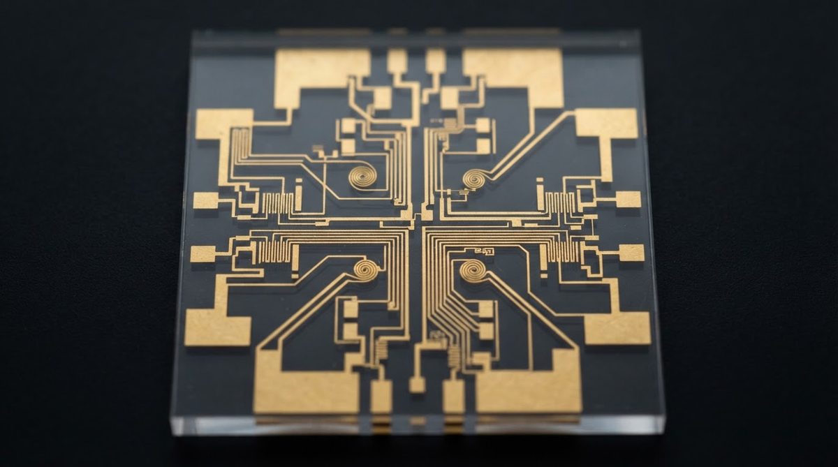
The term “quartz substrate” covers two fundamentally different materials. Fused silica is amorphous SiO₂ produced by melting high-purity quartz sand or synthesizing from SiCl₄. It is isotropic: dielectric constant, CTE, and optical transmission are the same in every direction. Most RF, photonic, and microfluidic substrates use fused silica.
Crystalline quartz is a single-crystal form with a well-defined lattice. It is anisotropic and piezoelectric. SAW (surface acoustic wave) filters, quartz crystal oscillators, and certain MEMS resonators require specific crystal cuts (AT-cut, ST-cut, Z-cut) because performance depends on orientation relative to the crystal axes. If your application does not exploit the piezoelectric effect or a specific crystal orientation, fused silica is almost always cheaper and easier to source.
Quartz Substrate Properties — Spec Table
| Parameter | Fused Silica | Crystalline Quartz (Z-cut) | Unit | Condition | Source |
|---|---|---|---|---|---|
| Dielectric constant (εr) | 3.75–3.82 | 4.52 (∥ c-axis) / 4.64 (⊥ c-axis) | — | 1 MHz, 25 °C | CoorsTek / IEEE Std 176 |
| Loss tangent (tan δ) | < 0.0001 | ~0.0001 | — | 1 MHz, 25 °C | CoorsTek |
| Thermal conductivity | 1.3–1.5 | 6.2–10.4 (orientation-dependent) | W/m·K | 25 °C | Heraeus / Kyocera |
| CTE | 0.5–0.55 | 7.1 (⊥ c) / 13.2 (∥ c) | ×10⁻⁶/°C | 20–300 °C | Heraeus Conamic |
| Flexural strength | 50–70 | ~100 | MPa | ASTM C1161 | CoorsTek |
| Max continuous use temp | 1050–1100 | ~573 (α→β transition) | °C | In air | Heraeus / general literature |
| UV cutoff (50% T, 1 mm) | ~180 | ~150 | nm | — | Heraeus Suprasil |
| Resistivity | > 10¹⁸ | > 10¹⁶ | Ω·cm | 25 °C | CoorsTek |
Typical values for commercially available material, for comparison only. Confirm against the datasheet for your specific grade.
The standout numbers are the near-zero CTE of fused silica and the extremely low loss tangent. Together they explain why fused silica dominates precision photomask blanks, optical flats, and millimeter-wave test fixtures where phase stability matters.
Where Quartz Substrates Are Used
RF and Microwave Circuits
At frequencies above 10 GHz, substrate loss becomes a primary limiter of filter Q-factor and insertion loss. Fused silica’s tan δ below 0.0001 keeps conductor loss dominant rather than dielectric loss, which is the designer’s goal. Thin-film metallization (Ti/Au, Cr/Au, or Ti/Pt/Au) is sputtered directly onto polished fused silica for microstrip and coplanar waveguide structures. If your design also needs thick-film silver metallization, note that silver paste firing temperatures (850 °C+) are compatible with fused silica but require careful profile control to avoid devitrification.
UV and Optical Applications
Fused silica transmits efficiently down to ~180 nm, making it the standard substrate for UV-C LED packages, excimer laser optics, and fluorescence biosensors. High-purity synthetic grades (e.g., Heraeus Suprasil) push the cutoff even lower. For UV-C LED packaging specifically, aluminum nitride is often chosen for the thermal path while quartz or sapphire serves as the optical window. Compare this with sapphire substrates for electronics, which transmit well above ~200 nm but absorb below that.
MEMS and SAW Devices
Single-crystal quartz is the backbone of SAW filters used in every mobile phone’s RF front end. The piezoelectric coupling coefficient and temperature coefficient of frequency (TCF) depend on the crystal cut. AT-cut quartz, for example, achieves near-zero TCF around 25 °C, which is why it dominates timing references. MEMS pressure sensors and gyroscopes also exploit quartz’s piezoelectric response and mechanical Q-factor.
Photomask Blanks and Semiconductor Tooling
The near-zero CTE of fused silica means a 6″ × 6″ × 0.25″ photomask blank changes less than 0.1 µm across a 10 °C temperature swing. No other commonly available substrate material matches this dimensional stability, which is why every advanced lithography mask is made on synthetic fused silica.
Worked Example: Dielectric Loss Comparison at 28 GHz
Consider a 50 Ω microstrip line, 10 mm long, on a 0.25 mm substrate at 28 GHz. The dielectric attenuation per unit length is approximated by:
α_d = (π × f × √εr_eff × tan δ) / c
For fused silica (εr ≈ 3.78, tan δ ≈ 0.0001): α_d ≈ 0.0057 dB/mm → 0.057 dB over 10 mm.
For 96% alumina (εr ≈ 9.6, tan δ ≈ 0.0002): α_d ≈ 0.018 dB/mm → 0.18 dB over 10 mm.
Fused silica delivers roughly 3× lower dielectric loss in this scenario. The actual total loss includes conductor loss, which depends on metallization, but the substrate contribution is significantly smaller on quartz.
Available Sizes and Thicknesses
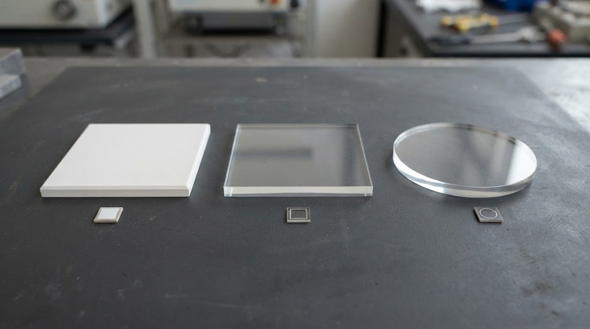
Fused silica substrates ship as rectangular coupons (10 × 10 mm up to 150 × 150 mm) and round wafers (2″, 3″, 4″, 6″, 8″ diameter). Thicknesses commonly range from 0.1 mm to 3.0 mm. Consult the ceramic substrate thickness chart for standard stock dimensions. Custom shapes are possible via laser cutting or diamond dicing, though fused silica is more chip-prone than alumina during mechanical processing.
When NOT to Use a Quartz Substrate
Quartz is the wrong material if any of these apply:
- You need to dissipate heat. At 1.3–1.5 W/m·K, fused silica is essentially a thermal insulator. Power LEDs, power transistors, and anything above ~0.5 W on a small footprint should use alumina, AlN, or Si₃N₄ instead.
- Your budget is tight and volumes are high. Fused silica substrates cost 3–10× more per cm² than 96% alumina, depending on grade and surface finish. For commodity sensor boards, alumina or even borosilicate glass substrates may suffice.
- You need mechanical toughness. Fused silica’s flexural strength (50–70 MPa) is less than half that of 96% alumina (300–380 MPa). Boards subject to clamping loads, vibration, or handling abuse will crack.
- Thick-film resistors are part of your circuit. Standard thick-film resistor pastes are formulated for alumina. They can fire on quartz, but sheet resistance values shift and TCR behavior changes. Qualification is required.
Quartz vs. Other Low-Loss Substrates
| Parameter | Fused Silica | Sapphire | Rogers RO4003C | 96% Alumina |
|---|---|---|---|---|
| εr (1 MHz) | 3.78 | 9.4–11.6 | 3.38 | 9.4–9.6 |
| tan δ (10 GHz) | < 0.0001 | ~0.00003 | 0.0027 | 0.0002 |
| CTE (ppm/°C) | 0.55 | 5.0–6.6 | 11 | 7.2 |
| Thermal cond. (W/m·K) | 1.4 | 25–46 | 0.71 | 24–28 |
| Max use temp (°C) | 1050 | 1800 | 250 | 1600 |
| Relative cost (per cm²) | High | Very high | Moderate | Low |
Typical values for commercially available material, for comparison only. Confirm against the datasheet for your specific grade.
If you need both low loss and thermal conductivity, sapphire wins but at a steep price premium. Rogers laminates are easier to process with standard PCB tooling but cannot survive temperatures above ~250 °C and have much higher dielectric loss than quartz.
Frequently Asked Questions
Can you metallize a quartz substrate with standard PCB processes?
Not with standard etched-copper PCB processes. Quartz substrates are metallized using thin-film sputtering (Ti/Au, Cr/Au) or thick-film screen printing (Ag, Au). Electroless plating is also possible with proper surface activation. Standard copper-clad lamination does not work because there is no adhesive prepreg system rated for quartz’s CTE.
Is fused silica the same as fused quartz?
They are both amorphous SiO₂ but differ in purity and production method. Fused quartz is made by melting natural quartz sand and retains trace impurities (Al, Na, OH). Fused silica is synthesized from gaseous precursors (SiCl₄) and achieves higher purity, lower UV absorption, and lower fluorescence. For electronics substrates, either grade can work; for UV-C optics below 200 nm, synthetic fused silica is required.
What surface finish can I get on a quartz substrate?
Optical-grade polishing to Ra < 0.5 nm (per interferometric measurement) is standard for photomask blanks and epi-ready wafers. For RF circuits, a fine-ground or polished finish with Ra < 50 nm is typical. Lapped finishes (Ra 0.2–0.8 µm) are available for less critical applications at lower cost.
Does quartz outgas in vacuum?
Fused silica has very low outgassing rates after a moderate bakeout (150 °C, 24 h). Water adsorbed on the surface is the primary volatile; bulk outgassing of SiO₂ is negligible below 800 °C. This makes quartz substrates suitable for vacuum packaging and space-qualified assemblies, per NASA ASTM E595 screening (TML < 1.0%, CVCM < 0.1%).
How does quartz compare to borosilicate glass for RF?
Borosilicate glass (e.g., Schott Borofloat 33) has a loss tangent around 0.0037 at 1 MHz—roughly 37× higher than fused silica. At frequencies above a few GHz, the difference becomes significant. Quartz is the better choice for any circuit where dielectric loss directly affects system performance. For lower-frequency or cost-sensitive sensor substrates, borosilicate may be adequate.
Next Step
If your design calls for a quartz substrate in a specific size, thickness, or with metallization, you can request a custom-shape ceramic substrate quote. To compare quartz against alumina or sapphire side by side with samples in hand, consider ordering a ceramic substrate sample kit.