A metallized ceramic substrate is a ceramic base—typically alumina (Al₂O₃), aluminum nitride (AlN), or silicon nitride (Si₃N₄)—with a patterned metal layer that carries current, dissipates heat, or provides a solderable surface. The three metals used in nearly every commercial design are copper (Cu), silver (Ag), and gold (Au). Each brings a distinct balance of electrical conductivity, thermal performance, adhesion strength, and cost. Choosing the right one depends on your operating environment, frequency range, and budget.
Key Takeaways
- Copper offers the best bulk thermal conductivity (≈ 400 W/m·K) and the lowest cost per unit area, but it oxidizes readily and requires barrier or protective finishes.
- Silver has the highest electrical conductivity of any metal (6.3 × 10⁷ S/m at 20 °C per CRC Handbook) and is the standard for thick-film RF and microwave circuits.
- Gold resists oxidation and corrosion indefinitely, making it the default for wire-bondable pads, hermetic packages, and harsh-environment electronics.
- Metallization method matters as much as metal choice: thick film, thin film, DBC, DPC, and AMB each impose different thickness ranges, adhesion strengths, and minimum feature sizes.
- No single metal is best for every application; many designs combine two metals on the same substrate (e.g., copper planes for heat spreading with gold bond pads).
How Metal Gets onto Ceramic: Process Overview
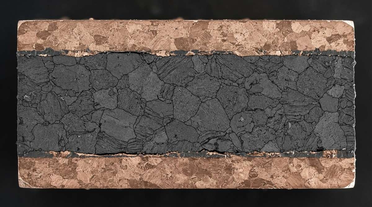
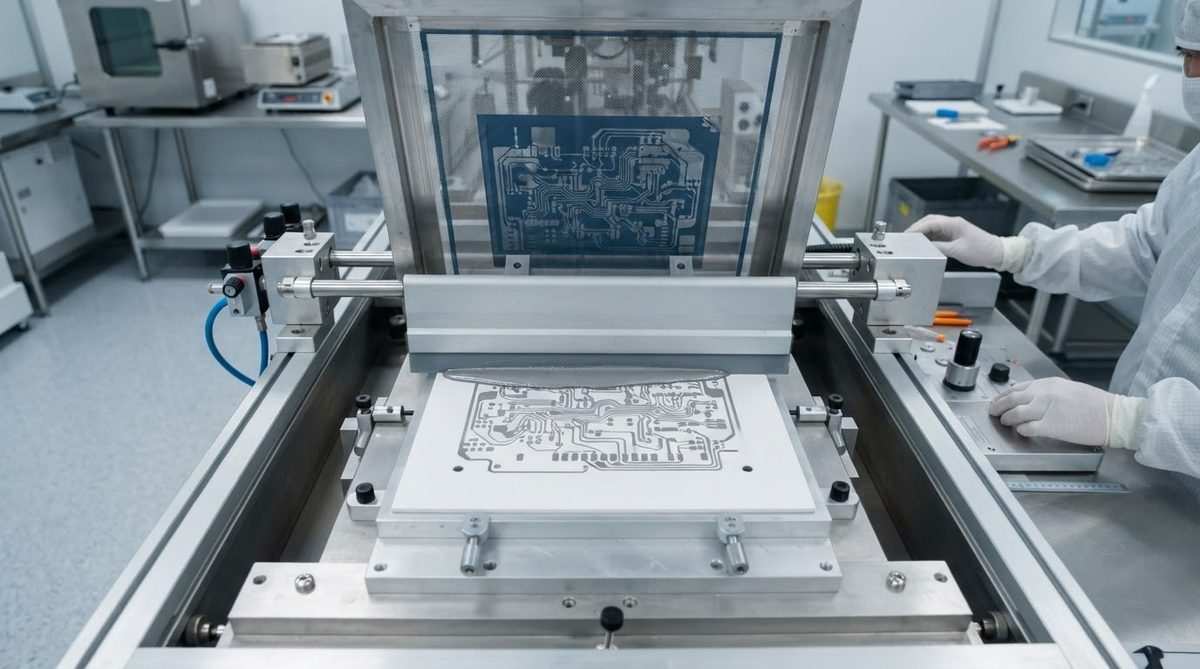
The metallization process determines the metal’s thickness, adhesion, line resolution, and cost. Five processes account for nearly all production substrates.
Thick film uses screen-printed metal-glass pastes fired at 850–1000 °C. It is the most common route for silver and gold conductors on alumina. Typical conductor thickness is 8–15 µm, and minimum line/space is around 100–125 µm. The glass frit in the paste bonds chemically to the ceramic surface, producing adhesion strengths of 20–40 N/mm² (per DuPont 6142D datasheet). Thick-film silver and gold pastes are available from Heraeus, DuPont, and ESL.
Thin film deposits metal by sputtering or evaporation, followed by photolithographic patterning and electroplating. Total metal thickness ranges from sub-micron seed layers up to 5–10 µm after plating. Line/space resolution reaches 10–25 µm, which makes thin film the choice for high-density interconnects and precision resistor networks. Common thin-film stacks include Ti/Pt/Au, Ti/Cu/Ni/Au, and Cr/Ni/Au. Alumina 96% thin-film substrates are the workhorse here.
DBC (Direct Bonded Copper) bonds a copper foil (typically 127–500 µm thick) to the ceramic using a copper-oxide eutectic at approximately 1065 °C. This produces very thick copper layers with excellent thermal conductivity. DBC is limited to oxide-forming ceramics—primarily alumina and, with process modifications, AlN. See alumina 96% DBC substrates for specifications.
DPC (Direct Plated Copper) combines sputtered seed layers with electroplated copper, reaching 1–100 µm thickness with finer features than DBC—typically 50–75 µm line/space. It works on both alumina and AlN. Alumina DPC substrates are widely used in LED and power electronics.
AMB (Active Metal Brazing) uses a titanium-containing braze alloy (e.g., AgCuTi) to bond copper foil to ceramics that resist oxide bonding, especially Si₃N₄ and AlN. Copper thickness is similar to DBC (150–800 µm), and the brazed joint is mechanically stronger, which matters for power-cycling reliability. AMB ceramic substrates are increasingly specified in EV traction inverters.
Copper, Silver, and Gold: Property Comparison
| Parameter | Copper (Cu) | Silver (Ag) | Gold (Au) | Unit | Condition / Source |
|---|---|---|---|---|---|
| Electrical resistivity | 1.68 | 1.59 | 2.44 | µΩ·cm | 20 °C, bulk; CRC Handbook of Chemistry and Physics, 97th ed. |
| Thermal conductivity | 400 | 429 | 317 | W/m·K | 20 °C, bulk |
| Melting point | 1085 | 962 | 1064 | °C | — |
| CTE | 16.5 | 18.9 | 14.2 | ppm/°C | 20–300 °C |
| Oxidation in air | Forms CuO above ~200 °C | Tarnishes (Ag₂S) in sulfur-containing atmospheres | Negligible | — | — |
| Wire bondability | Poor without finish | Poor | Excellent (Au and Al wire) | — | MIL-STD-883, Method 2011 |
| Solderability (SAC305) | Good with Ni barrier | Good, but Ag leaching risk | Good, but Au embrittlement above ~3 wt% | — | IPC J-STD-001 |
| Relative raw material cost | 1× | ~0.8–1.2× | ~50–80× | — | Approximate, varies with commodity markets |
Typical values for commercially available material, for comparison only. Confirm against the datasheet for your specific grade.
When to Choose Each Metal
Copper: Power Electronics and Thermal Management
Copper is the default for any design where current-carrying capacity or heat spreading is the primary concern. DBC and AMB substrates carry 150–500 µm of copper, handling hundreds of amps per centimeter of trace width. In power modules (IGBTs, SiC MOSFETs), the substrate’s copper layer doubles as both the electrical conductor and the primary thermal path between the die and the heatsink.
The main drawback is oxidation. Bare copper surfaces degrade within hours in humid air and cannot be wire-bonded reliably. Every copper-metallized substrate needs a protective finish: ENIG, ENEPIG, electroplated Ni/Au, or at minimum an OSP (organic solderability preservative) for short shelf life. Factor this finishing step into cost and lead time.
Silver: RF, Microwave, and Thick-Film Circuits
Silver’s low resistivity and mature thick-film paste ecosystem make it dominant in hybrid microstrip and stripline circuits from 1 GHz through millimeter-wave frequencies. Thick-film silver on 96% alumina is the standard construction for radar T/R modules, satellite filters, and telecom duplexers. For more detail, see thick-film silver metallized ceramic substrates.
Silver migration is the chief reliability risk. Under DC bias in humid conditions, silver ions migrate between adjacent conductors, eventually forming dendrites that short the circuit. Mitigation strategies include glass encapsulation, conformal coating, and palladium-silver (PdAg) alloy pastes, which reduce migration at the cost of higher resistivity (~3–5 µΩ·cm vs. 1.59 µΩ·cm for pure Ag).
Gold: Wire Bonding, Hermetic Packages, and Harsh Environments
Gold is chosen when the surface must remain pristine over years of storage or operation without protective coatings. Thick-film gold on alumina is the baseline for hybrid microcircuit packages per MIL-PRF-38534. Thin-film Ti/Pt/Au or Cr/Ni/Au stacks serve as under-bump metallization for flip-chip die attach. Gold-metallized ceramic substrates are non-negotiable for Class K (space-grade) and implantable medical devices where long-term hermeticity is required.
The obvious trade-off is cost. At current commodity prices, gold is roughly 50–80× more expensive than copper per unit weight. Designs minimize gold usage by applying it only where needed—bond pads and seal rings—while running copper or silver for the bulk conductor pattern.
Worked Example: Thermal Resistance of a Copper-Metallized AlN Substrate
Suppose you need to mount a 10 W SiC diode on an AlN substrate with 300 µm DBC copper on each side. The die footprint is 3 mm × 3 mm, and the ceramic is 0.635 mm thick.
Step 1: Copper layer thermal resistance.
RCu = t / (k × A) = 0.0003 m / (400 W/m·K × 9 × 10⁻⁶ m²) = 0.083 °C/W
Step 2: AlN ceramic thermal resistance.
RAlN = 0.000635 m / (170 W/m·K × 9 × 10⁻⁶ m²) = 0.415 °C/W
(Using 170 W/m·K, lower bound for commercial AlN per Kyocera SH-170 datasheet.)
Step 3: Total substrate stack (top Cu + AlN + bottom Cu).
Rtotal = 0.083 + 0.415 + 0.083 = 0.581 °C/W
Step 4: Temperature rise at 10 W.
ΔT = 10 W × 0.581 °C/W = 5.8 °C across the substrate stack.
If you switched the same geometry to 96% alumina (k ≈ 24 W/m·K), the ceramic layer alone would contribute 2.94 °C/W, pushing the total to 3.11 °C/W and a 31 °C rise. That difference is why copper-metallized AlN substrates are standard in high-power SiC and GaN modules.
Matching Metal to Ceramic Material
| Ceramic | Compatible Metallization Processes | Typical Metals | Notes |
|---|---|---|---|
| Al₂O₃ 96% | Thick film, thin film, DBC, DPC, AMB | Cu, Ag, Au, PdAg | Most versatile; accepts all standard processes |
| Al₂O₃ 99.6% | Thin film, thick film | Au, Cu, Ag | Higher purity gives smoother surface for thin film; see 99.6% alumina thin-film substrates |
| AlN | DBC (with oxidation pre-treatment), DPC, AMB, thin film, thick film (limited) | Cu, Au | Ag thick-film pastes on AlN are uncommon; Cu dominates for power |
| Si₃N₄ | AMB | Cu (via AgCuTi braze) | Highest fracture toughness; preferred for EV power modules |
| BeO | Thick film, thin film | Au, Cu | Beryllium oxide dust is a confirmed carcinogen causing chronic beryllium disease. Restricted use; consult safety data before specifying. |
Typical values for commercially available material, for comparison only. Confirm against the datasheet for your specific grade.
When NOT to Use Metallized Ceramic
Large-area, low-power boards. If your circuit runs below 1 W, operates under 125 °C, and exceeds 100 cm² in area, FR-4 or metal-core PCB (MCPCB) will cost a fraction of ceramic and meet your needs.
Frequent design iterations. Thick-film screens and thin-film photomasks add NRE cost and 1–3 weeks of lead time per revision. If you are still iterating weekly, prototype on FR-4 first and move to ceramic once the layout is frozen.
High-frequency designs above 77 GHz on lossy substrates. At millimeter-wave frequencies, 96% alumina’s loss tangent (tan δ ≈ 0.0002–0.001 at 10 GHz, per CoorsTek ADS-96R datasheet) may still be acceptable, but fused quartz substrates (tan δ ≈ 0.00005) or LTCC may outperform it. Evaluate your link budget before defaulting to alumina.
Extreme mechanical shock. Ceramic is brittle. If your product faces repeated drop impacts (consumer handhelds, field-deployed sensors), consider flex-rigid PCBs or MCPCB with mechanical damping.
Frequently Asked Questions
Can I solder directly to a metallized ceramic substrate?
Yes, provided the metallization is solderable. Thick-film silver and gold accept standard SAC305 or SnPb solder. Bare copper requires a nickel barrier (3–5 µm) to prevent copper dissolution into the solder. Always verify wettability with your specific paste and reflow profile.
What adhesion strength should I expect?
Thick-film conductors on 96% alumina typically achieve 20–40 N/mm² peel strength, measured per ASTM F1842. Thin-film stacks with a Ti or Cr adhesion layer reach 30–60 N/mm². DBC copper adhesion exceeds 80 N/mm² because the bond is a copper-oxide eutectic, not a deposited interface.
Does silver migration affect all silver-metallized substrates?
Silver migration requires three conditions simultaneously: DC bias, moisture, and an ionic transport path. In hermetically sealed packages or low-humidity environments, pure silver conductors can operate reliably for decades. For unsealed assemblies in humid conditions, use PdAg alloy paste or apply a glass overglaze to suppress migration.
How thick can copper be on a ceramic substrate?
DBC and AMB processes bond copper foils from 127 µm (5 mil) up to 800 µm (31 mil). DPC electroplating typically reaches 1–100 µm. Thin-film sputtered copper is usually under 5 µm before plating. The right thickness depends on your current density and thermal requirements.
Can I combine two metals on one substrate?
Yes, and it is common practice. A typical power module uses thick copper planes for heat spreading and adds a thin Ni/Au finish on bond-pad areas for wire bonding. Similarly, RF hybrids may use silver conductors with gold bond pads deposited in a second print-and-fire step.
Where can I find datasheets for specific metallized substrate products?
Datasheets for alumina, AlN, and other ceramic substrates with various metallization options are available in the ceramic substrate datasheet library. Each datasheet lists conductor thickness, adhesion, sheet resistance, and recommended soldering profiles.
Next Step
If you have identified your metal and process combination, the next step is confirming that your substrate size and thickness are available. Check the ceramic substrate thickness chart for standard options, or request a quote for custom dimensions.