Ceramic substrate datasheets are the starting point for any design that depends on precise thermal, dielectric, or mechanical performance. This page collects the key property values for the most common ceramic substrate materials and metallization processes, presented with units, test conditions, and sources so you can drop them straight into your thermal model or material-selection matrix.
Key Takeaways
- 96% alumina (Al₂O₃) offers 24–28 W/m·K thermal conductivity at 20 °C and is the lowest-cost ceramic substrate option.
- 99.6% alumina raises thermal conductivity to 28–35 W/m·K and improves surface finish for thin-film metallization.
- Aluminum nitride (AlN) reaches 170–200 W/m·K at 20 °C, making it the preferred choice for high-power-density designs.
- The metallization process (thick film, thin film, DBC, DPC, AMB) determines copper thickness range, adhesion strength, and minimum trace/space — not the ceramic alone.
- Always confirm datasheet values against the specific grade and supplier lot; published ranges are typical, not guaranteed.
How to Read a Ceramic Substrate Datasheet
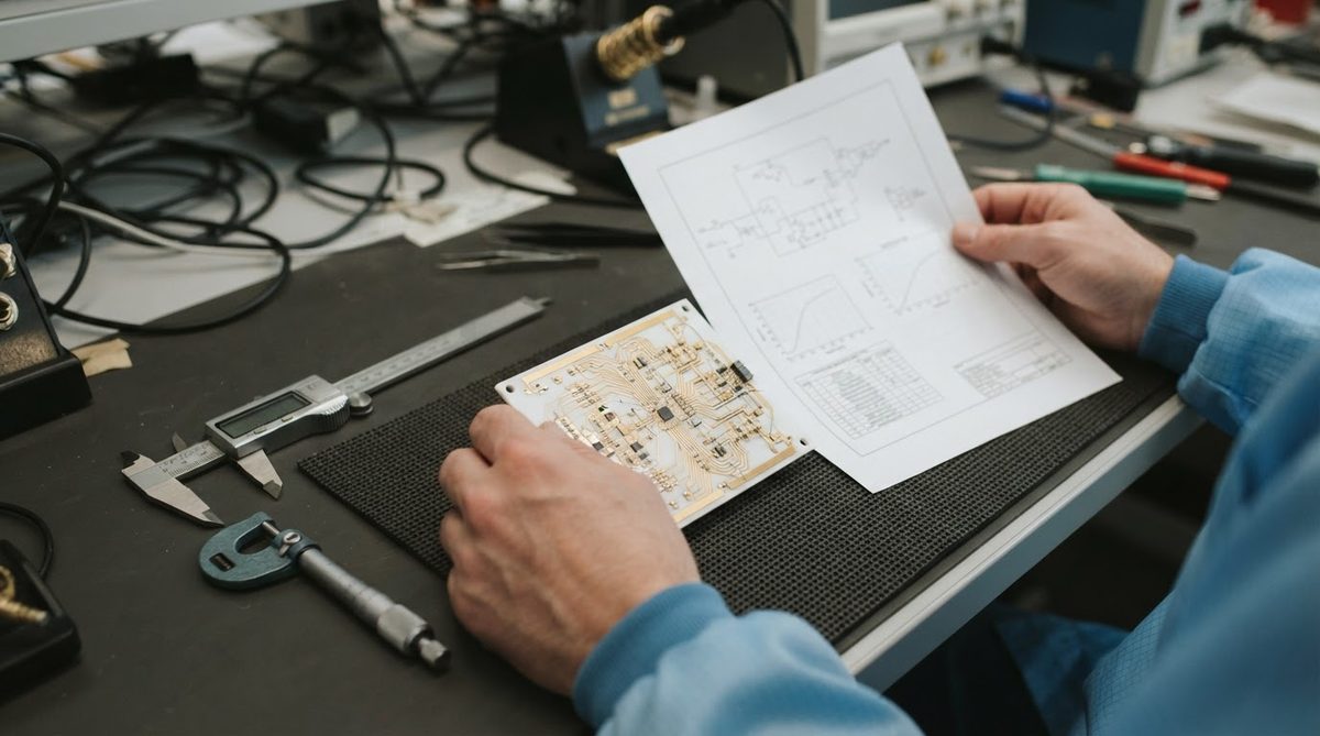
A ceramic substrate datasheet reports two categories of data: bulk ceramic properties and metallized-assembly properties. Bulk properties — thermal conductivity, flexural strength, dielectric constant — belong to the ceramic itself and are set during sintering. Assembly properties — peel strength, copper thickness, trace resolution — depend on the metallization process applied to that ceramic.
Confusing the two leads to specification errors. A 96% alumina substrate has the same thermal conductivity whether it carries thick-film or DPC metallization, but its minimum trace width differs by an order of magnitude between those two processes. When you review a datasheet, check which layer of the stack each number describes.
Pay attention to test conditions. Thermal conductivity for AlN, for example, drops measurably above 200 °C. A single value stated without a temperature is incomplete. The tables below include conditions and source references so you can trace each number back.
Ceramic Substrate Material Properties — Comparison Table
| Parameter | Al₂O₃ 96% | Al₂O₃ 99.6% | AlN | Unit | Condition | Source |
|---|---|---|---|---|---|---|
| Thermal conductivity | 24–28 | 28–35 | 170–200 | W/m·K | 20 °C | CoorsTek, Kyocera datasheets |
| CTE | 6.5–7.2 | 6.7–7.4 | 4.4–4.7 | ppm/°C | 20–300 °C | Kyocera, Maruwa datasheets |
| Dielectric constant (εr) | 9.0–9.5 | 9.7–9.9 | 8.5–9.0 | — | 1 MHz, 20 °C | CoorsTek, CeramTec datasheets |
| Dielectric strength | 10–15 | 12–16 | 14–17 | kV/mm | AC, 20 °C | CoorsTek datasheets |
| Flexural strength | 300–380 | 350–450 | 300–400 | MPa | ASTM C1161, 20 °C | CoorsTek, Kyocera datasheets |
| Density | 3.72–3.78 | 3.86–3.92 | 3.25–3.30 | g/cm³ | 20 °C | Maruwa, CoorsTek datasheets |
| Max continuous use temp. | 1 600 | 1 700 | 1 000 (in inert atm.) | °C | Manufacturer recommendation | Kyocera, CeramTec datasheets |
Typical values for commercially available material, for comparison only. Confirm against the datasheet for your specific grade.
Datasheets by Material and Metallization Process
96% Alumina Substrates
96% alumina is the workhorse ceramic substrate. It is available across the widest range of metallization processes: 96% Al₂O₃ thick film for standard hybrid circuits, 96% Al₂O₃ DPC for fine-line patterning down to 30–50 µm trace/space, and 96% Al₂O₃ DBC for power modules requiring 0.2–0.6 mm bonded copper. Each product page includes a downloadable datasheet with the full specification set for that combination.
For co-fired designs, 96% alumina is also processed as LTCC, where the ceramic and conductors are laminated and sintered together. The resulting substrate has embedded vias and internal conductor layers, but the bulk ceramic properties shift slightly due to the glass content in the tape system.
99.6% Alumina Substrates
Higher purity alumina improves thermal conductivity by roughly 20–30% over the 96% grade and produces a smoother as-fired surface (Ra < 0.3 µm typical). This makes it the preferred base for thin-film metallization, where sputtered or evaporated metal layers demand sub-micron surface quality. See the 99.6% Al₂O₃ thin film substrate datasheet for surface roughness, adhesion, and resistor tolerance specifications.
Aluminum Nitride (AlN) Substrates
AlN’s thermal conductivity of 170–200 W/m·K makes it the go-to substrate for IGBT modules, high-brightness LED arrays, and RF power amplifiers where heat flux exceeds what alumina can handle. Its CTE of 4.4–4.7 ppm/°C is a close match to silicon (2.6 ppm/°C) and SiC (4.0 ppm/°C), reducing solder-joint fatigue in power cycling. The AlN DBC substrate datasheet covers copper thickness options, bond strength per IPC-TM-650, and thermal resistance per unit area.
Which Datasheet Parameters Matter Most
Not every line on a datasheet carries equal weight for every application. Here is a quick decision guide:
- Power electronics (IGBTs, SiC MOSFETs): Prioritize thermal conductivity, CTE match to die, copper thickness, and partial-discharge inception voltage.
- RF and microwave: Focus on dielectric constant (εr), loss tangent (tan δ), and surface roughness. A 0.5 shift in εr changes a microstrip impedance by several ohms.
- High-reliability / aerospace: Flexural strength (per ASTM C1161), hermeticity, and thermal-shock resistance (ΔT cycles to failure) are the critical rows.
- LED thermal management: Thermal conductivity and reflectance at the emission wavelength. AlN outperforms alumina thermally, but 96% alumina with a white thick-film reflector layer may win on cost for lower-power arrays.
Worked Example — Using Datasheet Values in a Thermal Model
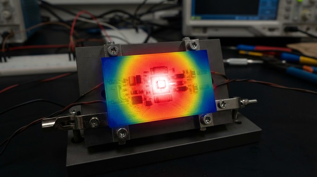
Suppose you need to estimate the thermal resistance through a 0.635 mm thick, 25 × 25 mm 96% alumina substrate under a power device dissipating 50 W.
Rth = t / (k × A)
Where t = 0.000635 m, k = 26 W/m·K (mid-range from the table above), A = 0.025 × 0.025 = 6.25 × 10⁻⁴ m².
Rth = 0.000635 / (26 × 6.25 × 10⁻⁴) = 0.039 °C/W.
At 50 W, the temperature drop across the substrate alone is about 2.0 °C. Switching to AlN (k ≈ 180 W/m·K) reduces that to roughly 0.28 °C — meaningful only if the total thermal stack is already tight. This is the kind of sanity check datasheet values enable before you commit to a more expensive material.
When a Ceramic Substrate Datasheet Is Not What You Need
If your design runs below 1 W/cm² heat flux and operates under 130 °C, standard FR-4 or metal-core PCB (MCPCB) datasheets will serve you at a fraction of the cost. Ceramic substrates add value when thermal conductivity above 20 W/m·K, dielectric strength above 10 kV/mm, or CTE matching to semiconductor die are genuine requirements — not nice-to-haves. Pulling a ceramic datasheet into a project that doesn’t need one wastes engineering time on tighter tolerances and longer lead times.
Similarly, if your primary concern is high layer count (>4 layers) with standard digital routing, organic substrates remain far more practical. Ceramic multilayer options (HTCC, LTCC) exist but are justified mainly by hermeticity, high-temperature operation, or embedded passives.
Request Physical Samples Alongside Datasheets
Numbers on a PDF only go so far. Surface finish, edge quality, and warpage are easier to evaluate with a substrate in hand. You can request a ceramic substrate sample kit to physically compare materials and processes before locking in your design.
FAQ
Are ceramic substrate datasheets standardized across manufacturers?
No. There is no single industry-wide template. Test methods are often referenced (ASTM, IEC, JIS), but the parameters reported and the conditions used vary by supplier. Always check which standard was used before comparing values from two different datasheets.
Can I use datasheet thermal conductivity directly in FEA?
Yes, as a starting input. Datasheet values are measured on bulk samples at a stated temperature (usually 20–25 °C). For accurate simulation at elevated temperatures, request temperature-dependent data from the substrate supplier or use published curves from sources like CoorsTek or Kyocera technical literature.
Do metallization processes change the ceramic’s bulk properties?
The bulk ceramic properties (thermal conductivity, CTE, εr) remain essentially unchanged by metallization. What changes are assembly-level properties: total thermal resistance through the copper-ceramic stack, peel strength, and achievable trace geometry. These are reported on the metallized-substrate datasheet, not the bare-ceramic datasheet.
What does “as-fired” surface roughness mean on a datasheet?
As-fired roughness is the surface finish straight out of the sintering furnace, with no post-processing. For 96% alumina, this is typically Ra 0.4–0.8 µm. Lapping or polishing can bring it below 0.1 µm, which is often required for thin-film deposition. The datasheet should state whether the roughness value is as-fired or polished.
How do I get a datasheet for a specific material-process combination?
Each product page on this site includes a downloadable datasheet for that exact combination. For example, the AlN DPC page provides thermal, electrical, and dimensional specs specific to direct-plated-copper on aluminum nitride. If you need a custom thickness or copper weight not listed, contact engineering directly.