A borosilicate glass substrate is a flat, polished sheet of borosilicate glass (typically Schott Borofloat 33 or Corning 7740/Pyrex equivalent) used as a base for thin-film circuits, MEMS devices, optical sensors, and RF components. Its defining advantages are a low coefficient of thermal expansion (3.25 ppm/K at 20–300 °C), optical transparency from UV through near-IR, and a dielectric constant of roughly 4.6 at 1 MHz. These properties make it a strong candidate for applications where alumina or FR-4 fall short on optical access or CTE matching to silicon.
Key Takeaways
- Borosilicate glass has a CTE of approximately 3.25 ppm/K (20–300 °C, per Schott Borofloat 33 datasheet), closely matching silicon’s 2.6 ppm/K.
- Thermal conductivity is only about 1.1 W/mK at 25 °C — roughly 20× lower than 96% alumina — so it is unsuitable for power dissipation.
- Dielectric loss tangent is around 37 × 10⁻⁴ at 1 MHz (Schott data), acceptable for moderate-frequency RF but higher than alumina or fused silica at millimeter-wave frequencies.
- Borosilicate glass is optically transparent (>90% transmission at 350–2500 nm), enabling through-substrate optical coupling.
- Mechanical strength is lower than alumina: flexural strength is roughly 25 MPa (per ASTM C158) versus 300+ MPa for 96% Al₂O₃.
Material Properties of Borosilicate Glass
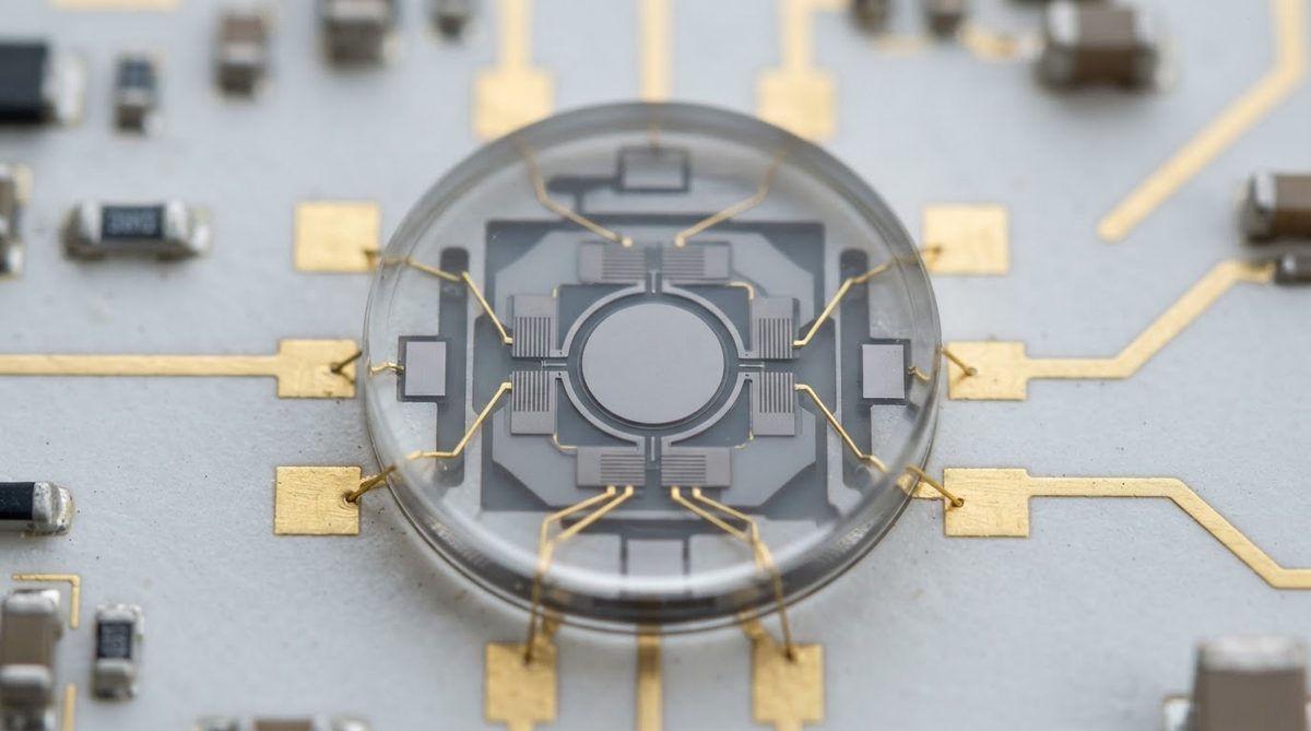
The table below compares borosilicate glass to two common ceramic substrates and fused silica. All values are for commercially available grades at room temperature unless stated otherwise.
| Parameter | Borosilicate Glass (Borofloat 33) | 96% Alumina (Al₂O₃) | Fused Silica | Unit | Source / Standard |
|---|---|---|---|---|---|
| CTE (20–300 °C) | 3.25 | 6.5–7.2 | 0.55 | ppm/K | Schott / CoorsTek datasheets |
| Thermal conductivity (25 °C) | 1.1 | 24–28 | 1.4 | W/mK | Schott / CoorsTek datasheets |
| Dielectric constant (1 MHz) | 4.6 | 9.0–9.5 | 3.8 | — | Schott / CoorsTek datasheets |
| Loss tangent (1 MHz) | 37 × 10⁻⁴ | 1–3 × 10⁻⁴ | 1 × 10⁻⁴ | — | Schott / Corning datasheets |
| Flexural strength | ~25 | 300–380 | ~50 | MPa | ASTM C158 / ASTM C1161 |
| Max continuous use temp. | 450–500 | 1600+ | 1000 | °C | Schott / CoorsTek datasheets |
| Optical transmission (visible) | >90% | Opaque | >90% | % at 500 nm | Schott / Corning datasheets |
| Volume resistivity (25 °C) | ~10¹² | ~10¹⁴ | ~10¹⁸ | Ω·cm | Schott / CoorsTek datasheets |
Typical values for commercially available material, for comparison only. Confirm against the datasheet for your specific grade.
The standout feature is CTE. At 3.25 ppm/K, borosilicate glass is much closer to silicon (2.6 ppm/K) than 96% alumina (6.5–7.2 ppm/K). This matters for die-attach reliability in MEMS packaging and flip-chip assemblies where thermal cycling stress at the bond interface drives failure. If your design requires an even closer CTE match to silicon, fused silica (0.55 ppm/K) is the next step, though it costs significantly more.
Typical Applications for Borosilicate Glass Substrates
MEMS packaging and anodic bonding. Borosilicate glass bonds directly to silicon wafers via anodic bonding at 300–450 °C. The close CTE match minimizes warpage and residual stress in pressure sensors, accelerometers, and microfluidic chips. This is probably the single largest use case for borosilicate glass substrates in electronics.
Optical and photonic assemblies. Transparency across the visible and near-IR spectrum allows through-substrate illumination or detection. Biosensor chips, waveguide couplers, and LED test carriers exploit this. Where you need a substrate that is both electrically insulating and optically transparent, glass is one of very few options.
RF test fixtures and low-frequency microwave. A dielectric constant of 4.6 and moderate loss tangent suit prototype RF test boards and antenna test fixtures up to a few GHz. Above roughly 10 GHz, the loss tangent of borosilicate glass climbs noticeably, and 99.6% alumina HTCC substrates or fused quartz become better choices.
Thin-film resistor networks and hybrid circuits. Glass surfaces can be polished to sub-nanometer Ra, supporting high-resolution sputtered thin-film metallization. Nichrome or tantalum nitride resistors deposited on glass achieve tight tolerance and low TCR.
Metallization Options on Borosilicate Glass
Borosilicate glass cannot be metallized the same way as alumina. Thick-film pastes fired at 850 °C would soften or deform the glass (strain point ~510 °C for Borofloat 33). The practical options are:
- Thin-film sputtering/evaporation — Ti/Pt/Au or Cr/Cu seed layers followed by electroplating. This is the standard route for MEMS and RF.
- Low-temperature thick-film pastes — Specialty polymer-based or low-fire glass-frit conductors cured below 450 °C. Conductivity is lower than standard thick-film silver or gold.
- Direct copper plating (semi-additive) — Seed layer plus pattern plating, similar to advanced PCB SAP processes. Achievable on glass but less mature than on ceramic.
If your circuit requires high-adhesion thick-film metallization or direct bonded copper (DBC), 96% alumina substrates are the established choice. For thin-film metallization on a transparent substrate, borosilicate glass works well.
Worked Example: CTE Mismatch Stress
Suppose you bond a 5 × 5 mm silicon die to a substrate and cycle from 25 °C to 150 °C (ΔT = 125 K). The shear strain at the bond interface is proportional to the CTE difference (Δα) times ΔT times the die half-diagonal.
For borosilicate glass: Δα = 3.25 − 2.6 = 0.65 ppm/K. Strain contribution ∝ 0.65 × 125 = 81 ppm.
For 96% alumina: Δα = 7.0 − 2.6 = 4.4 ppm/K. Strain contribution ∝ 4.4 × 125 = 550 ppm.
The alumina substrate produces roughly 6.8× more thermomechanical strain at the bond line. For MEMS devices with fragile silicon membranes, that difference often determines whether the part survives 1 000 thermal cycles. This is the core engineering reason to choose borosilicate glass over alumina in anodic-bonded MEMS.
When Not to Use a Borosilicate Glass Substrate
Power electronics or anything dissipating significant heat. At 1.1 W/mK, borosilicate glass is a thermal insulator. Even a few hundred milliwatts concentrated on a small die will create a large temperature rise. Use aluminum nitride substrates (170–200 W/mK) or alumina (24–28 W/mK) for thermal management.
High mechanical loads or vibration. Flexural strength around 25 MPa means glass substrates crack under loads that alumina or silicon nitride substrates (600–800 MPa) handle easily. Automotive or aerospace environments with shock and vibration are poor fits.
Millimeter-wave RF above 10 GHz. The loss tangent of borosilicate glass rises at higher frequencies. Fused silica, 99.6% alumina, or AlN are preferred for 5G mmWave, radar, and satellite uplink circuits.
High-temperature operation above 500 °C. The glass transition and softening behavior limits continuous use. Alumina substrates operate continuously above 1 600 °C.
Standard thick-film processing. If your production line uses 850 °C thick-film firing, borosilicate glass simply will not survive the furnace. Stick with alumina.
Borosilicate Glass vs. Sapphire Substrates
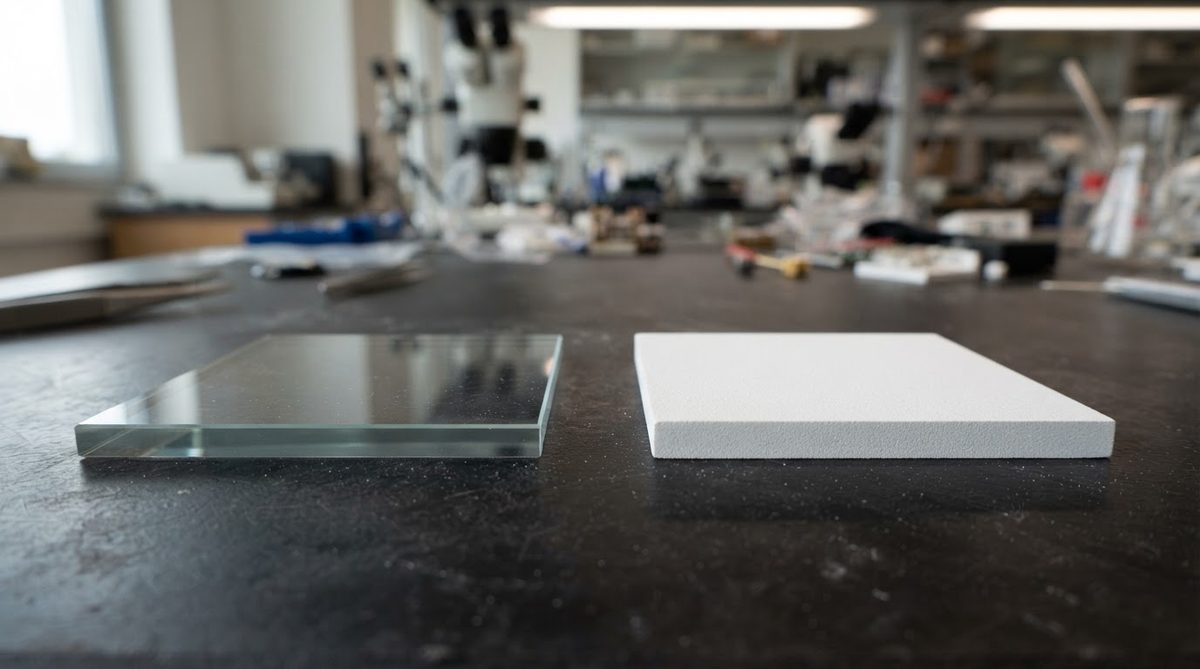
Both materials are optically transparent and electrically insulating. Sapphire substrates offer much higher thermal conductivity (~35 W/mK), superior hardness, and stability to 1 800 °C, but at significantly higher cost and with limited availability in large panel sizes. Borosilicate glass is far cheaper, available in large wafers and panels, and easier to drill, dice, and process. Choose sapphire when you need optical transparency plus thermal conductivity; choose borosilicate glass when cost, size, or anodic bonding compatibility drives the design.
Frequently Asked Questions
Can you anodically bond borosilicate glass to silicon?
Yes. Anodic bonding of borosilicate glass to silicon is a well-established MEMS process, typically performed at 300–450 °C with 200–1 000 V applied across the interface. The sodium ions in the glass migrate under the electric field, creating a strong hermetic seal. Schott Borofloat 33 and Corning 7740 are the standard grades for this process.
What surface finish (Ra) is available on borosilicate glass substrates?
Commercial borosilicate glass wafers are typically polished to Ra < 1 nm on one or both sides. Fire-polished float glass (Borofloat 33) achieves Ra around 0.5–1.0 nm without mechanical polishing. This surface quality supports fine-line thin-film metallization and direct wafer bonding.
Is borosilicate glass substrate the same as Pyrex?
Pyrex is a brand name originally referring to Corning 7740 borosilicate glass. Today the Pyrex brand is applied to different compositions depending on the manufacturer and region. For engineering substrates, specify the grade by number (e.g., Corning 7740, Schott Borofloat 33) rather than relying on the Pyrex name.
What is the maximum substrate size for borosilicate glass?
Schott produces Borofloat 33 in panels up to 1 200 × 1 200 mm and wafers up to 300 mm diameter. Practical substrate sizes depend on your metallization and dicing equipment. For standard ceramic substrate sizes and custom panels, check availability with your supplier.
Can you laser-drill vias in borosilicate glass?
Yes. UV and ultrafast (femtosecond) lasers drill clean vias in borosilicate glass down to roughly 10–25 µm diameter. Through-glass vias (TGVs) filled with copper are used in advanced interposers and 3D packaging. The process is more specialized and costly than via drilling in alumina.
Next Step
If your application needs optical transparency and a close CTE match to silicon, borosilicate glass is worth evaluating. For designs where thermal conductivity, mechanical strength, or thick-film metallization are priorities, alumina or aluminum nitride substrates are the better path. To compare substrate options or request samples, visit the ceramic substrate sample kit page.