Aluminum nitride (AlN) substrates offer thermal conductivity of 170–230 W/mK—roughly 6–8× higher than 96% alumina—while maintaining electrical resistivity above 1012 Ω·cm. If your design dissipates more than a few watts per square centimeter and you need an electrically insulating carrier, AlN is the default choice. This page covers what you need to specify when you buy aluminum nitride substrates, which grades and metallization options exist, and how to avoid the most common sourcing mistakes.
Key Takeaways
- Commercial AlN substrates are available in two broad thermal conductivity tiers: 170–180 W/mK (standard) and 200–230 W/mK (high-purity), per datasheets from Maruwa and Kyocera.
- CTE of AlN (4.5–4.7 ppm/°C at 20–400 °C) closely matches silicon (3.5–4.1 ppm/°C), reducing die-attach stress in power and RF modules.
- Metallization method—DBC, AMB, DPC, thick film, or thin film—determines copper thickness range, minimum trace/space, and maximum operating temperature.
- AlN is moisture-sensitive during storage and processing; unmetallized substrates should be kept in nitrogen-purged packaging or used within 24–48 hours of exposure to ambient humidity.
- Cost runs 3–5× higher than equivalent 96% Al₂O₃ substrates, driven primarily by sintering atmosphere (nitrogen vs. air) and raw-material purity.
AlN Substrate Grades: Standard vs. High-Purity
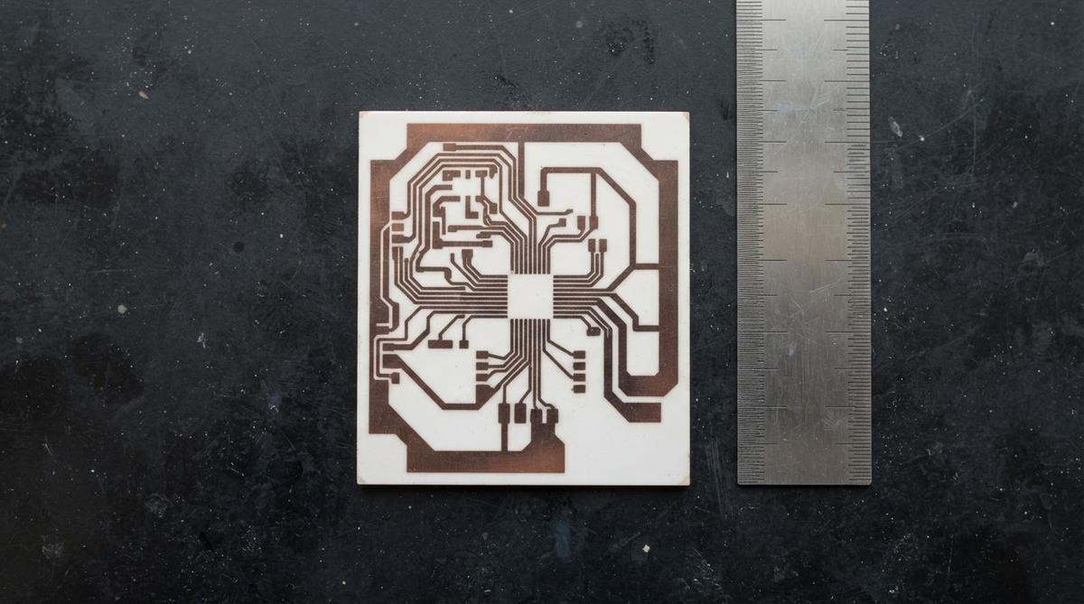
The single most important spec when you buy an AlN substrate is thermal conductivity grade. Two tiers dominate the market:
| Parameter | Standard Grade | High-Purity Grade | Unit | Condition | Source |
|---|---|---|---|---|---|
| Thermal conductivity | 170–180 | 200–230 | W/mK | 20 °C, laser flash per ASTM E1461 | Maruwa SH-30 / SH-50 datasheets |
| Flexural strength | 350–400 | 300–350 | MPa | 3-point bend per ASTM C1161 | Kyocera SH-170 / SH-200 datasheets |
| Dielectric strength | 15–17 | 15–17 | kV/mm | AC, 60 Hz | CoorsTek AlN datasheet |
| CTE | 4.5–4.7 | 4.5–4.7 | ppm/°C | 20–400 °C | Maruwa |
| Density | 3.26–3.30 | 3.30–3.33 | g/cm³ | Archimedes method | Kyocera |
| Dielectric constant (εr) | 8.5–8.9 | 8.5–8.9 | — | 1 MHz | CoorsTek |
Typical values for commercially available material, for comparison only. Confirm against the datasheet for your specific grade.
High-purity grades achieve higher thermal conductivity through tighter control of oxygen content in the AlN powder (below 0.8 wt%) and longer sintering dwell times. The trade-off is lower flexural strength and higher cost. For most power-electronics applications below 150 W/cm², standard-grade AlN at 170 W/mK is sufficient. Reserve 200+ W/mK grades for IGBT modules, high-power laser diodes, or RF amplifiers where every degree of junction temperature matters.
Metallization Options for AlN Substrates
Bare AlN substrates are useful for thermal spreaders and spacers, but most buyers need metallized substrates ready for die attach and wire bonding. The metallization process you choose dictates copper thickness, trace resolution, bond strength, and cost.
DBC (Direct Bonded Copper)
AlN DBC substrates bond a copper foil (typically 0.127–0.30 mm) to the ceramic through a copper-oxide eutectic reaction at around 1,065 °C. DBC suits power modules carrying tens to hundreds of amps. Minimum trace/space is typically 0.3–0.5 mm, so it is not the right process for fine-pitch circuits.
AMB (Active Metal Brazing)
For higher reliability under thermal cycling, AlN AMB substrates use a titanium-containing braze alloy (e.g., Ag-Cu-Ti) to join copper foil at 800–900 °C. AMB produces a stronger ceramic-to-copper interface than DBC—peel strength above 5 N/mm per IEC 60749-19—making it the preferred process for automotive-grade SiC and GaN power modules that endure –40 to +175 °C cycling.
DPC (Direct Plated Copper)
AlN DPC substrates use sputtered seed layers followed by electroplating to build up copper from 10 µm to about 100 µm. DPC achieves finer features—trace/space down to 50 µm or less—and tighter thickness uniformity than DBC. It is the go-to process for LED packages, RF hybrids, and sensor substrates where pattern density matters more than bulk current capacity.
Thick Film and Thin Film
AlN thick film substrates use screen-printed conductor pastes (tungsten, gold, or silver-palladium) fired at 850–950 °C. AlN thin film substrates deposit conductors by sputtering and photolithography, reaching trace widths below 25 µm. Thin film is common in mmWave and MMIC packaging where impedance control at 20–80 GHz is required.
Standard Sizes and What to Specify
AlN substrates are typically supplied as fired, lapped, or polished blanks in rectangular or circular formats. Common stock sizes include 50.8 × 50.8 mm, 114.3 × 114.3 mm, and 2″–4″ diameter wafers. Thicknesses range from 0.25 mm to 1.0 mm; consult a ceramic substrate thickness chart for standard options.
When requesting a quote, specify at minimum:
- Thermal conductivity grade – 170 or 200+ W/mK.
- Dimensions and tolerances – length × width × thickness, plus position tolerance for any holes or cutouts.
- Surface finish – as-fired (Ra 0.4–0.8 µm), lapped (Ra 0.1–0.3 µm), or polished (Ra < 0.05 µm).
- Metallization – process (DBC, AMB, DPC, thick film, thin film), conductor material, and copper thickness.
- Quantity and schedule – prototype vs. production volumes affect tooling amortization.
Worked Example: Thermal Resistance of an AlN Substrate
Suppose you are mounting a 100 W SiC MOSFET die (10 × 10 mm footprint) on a 0.635 mm thick AlN substrate rated at 170 W/mK. The conduction thermal resistance through the substrate is:
Rth = t / (k × A) = 0.000635 m / (170 W/mK × 0.0001 m²) = 0.037 °C/W
For comparison, the same geometry in 96% alumina (25 W/mK) yields 0.254 °C/W—a 6.8× difference. At 100 W dissipation, that translates to a 21.7 °C lower temperature drop across the substrate with AlN. In a system where junction temperature is already near the 175 °C limit, that margin can be the difference between a passing and failing qualification.
When Not to Buy AlN
AlN is the wrong substrate if:
- Thermal load is modest. Below roughly 10 W/cm², 96% alumina at 24–28 W/mK often suffices and costs 3–5× less. See copper-metallized alumina substrates as an alternative.
- Mechanical shock and vibration dominate. AlN flexural strength (300–400 MPa) is adequate for most electronics, but silicon nitride (Si₃N₄) at 600–800 MPa is far tougher. For power modules in traction inverters, consider purchasing Si₃N₄ substrates instead.
- RF loss tangent matters more than thermal conductivity. At frequencies above 40 GHz, quartz (SiO₂) substrates offer a lower dielectric constant (3.8) and loss tangent (< 0.0001), which may outweigh AlN’s thermal advantage.
- Budget is the primary constraint. For LED assemblies under 3 W, metal-core PCBs (MCPCBs) at 1–3 W/mK with aluminum base plates cost a fraction of AlN and meet the thermal requirement.
Moisture Sensitivity: A Detail Most Buyers Miss
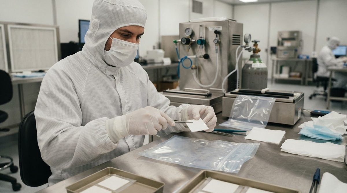
Unmetallized AlN reacts with moisture in ambient air, forming a thin layer of aluminum hydroxide on the surface. This layer degrades solder wetting and adhesion if the substrate is metallized or bonded after prolonged exposure. Industry best practice, per guidance in JEDEC J-STD-033D for moisture-sensitive components, is to store bare AlN substrates in nitrogen-purged, vacuum-sealed packaging and process them within 24–48 hours of opening. If substrates have been exposed longer, a 150 °C bake for 2–4 hours in a dry nitrogen environment can restore surface quality—but prevention is cheaper than rework.
Frequently Asked Questions
What is the lead time for AlN substrates?
Bare AlN blanks in standard sizes typically ship in 1–2 weeks. Metallized substrates with custom patterns require 3–5 weeks depending on the metallization process, pattern complexity, and quantity.
Can AlN substrates be laser-cut to custom shapes?
Yes. Laser scribing and cutting are the preferred methods for creating non-rectangular AlN parts, since mechanical routing risks edge chipping. Tolerances of ±0.05 mm are achievable with UV or CO₂ laser systems.
Is AlN compatible with lead-free solder?
AlN substrates with nickel/gold or nickel/palladium/gold surface finishes are fully compatible with SAC305 and other lead-free solder alloys. The key requirement is that the metallization stack provides a solderable barrier layer—typically electroless nickel at 3–5 µm plus immersion gold at 0.05–0.1 µm.
How does AlN compare to BeO for thermal performance?
Beryllium oxide (BeO) offers 250–300 W/mK, roughly 30–50% higher than high-purity AlN. However, BeO dust is a confirmed human carcinogen that causes chronic beryllium disease, and its use is restricted or banned in many jurisdictions. For new designs, AlN is the standard replacement. See our beryllia safety page for handling requirements if you are working with legacy BeO hardware.
What is the minimum order quantity?
MOQ depends on the supplier and whether you need bare blanks or metallized substrates. Many suppliers, including AluminaPCB, offer prototype quantities starting at single pieces for standard sizes. Custom tooling for metallization patterns may carry a one-time NRE charge.
Next Step
If you have a thermal design that points to AlN, the fastest path forward is to submit your substrate dimensions, thermal conductivity grade, and metallization requirements for a quote. Upload your drawing or Gerber files at AluminaPCB’s instant quote page and expect a response within one business day.
Last reviewed: 2025-07