Aluminum nitride AlN thick film ceramic substrates pair a base material with 170–200 W/mK thermal conductivity to screen-printed conductor, resistor, and dielectric layers fired at 850–950 °C. The result is a circuit-ready substrate that moves heat 6–8× faster than 96% alumina while keeping the design flexibility of thick film patterning. For engineers evaluating aluminum nitride AlN thick film ceramic options, these substrates are the standard choice when a power device or high-brightness LED needs both efficient heat spreading and moderate circuit complexity on a single ceramic piece.
Key Takeaways
- AlN thick film substrates deliver 170–200 W/mK thermal conductivity at 25 °C, compared with 24–28 W/mK for 96% Al₂O₃ (per Maruwa and Kyocera datasheets).
- Thick film metallization on AlN typically uses silver (Ag) or gold (Au) pastes fired at 850–950 °C; copper pastes require nitrogen atmosphere firing to prevent AlN oxidation.
- CTE of AlN (4.4–4.7 ppm/°C, 25–400 °C) closely matches silicon (3.5–4.1 ppm/°C) and SiC (4.0–4.5 ppm/°C), reducing solder-joint fatigue in die-attach applications.
- AlN is 3–5× more expensive per unit area than 96% alumina, so it is justified only when thermal performance or CTE matching is the binding constraint.
What Is Aluminum Nitride AlN Thick Film Ceramic Processing?
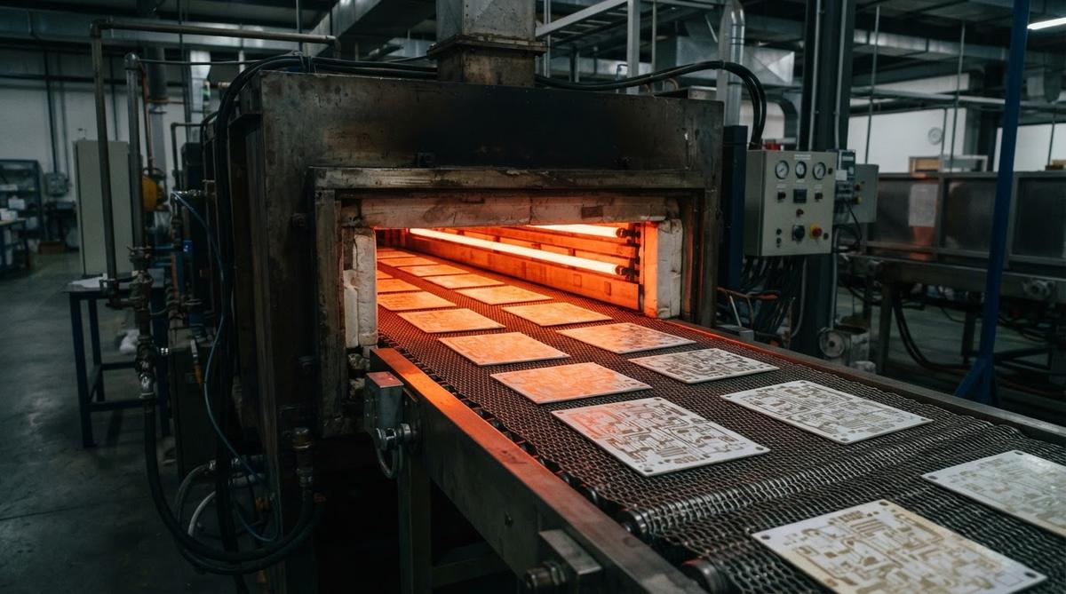
Thick film processing deposits conductor, resistor, and dielectric layers onto a fired ceramic substrate by screen printing metal-bearing pastes and then firing them in a belt furnace. On alumina, this is routine. On AlN, the process requires specific paste chemistries and a controlled atmosphere because AlN oxidizes above roughly 700 °C in air, forming an alumina surface layer that degrades both adhesion and thermal performance.
Most AlN-compatible thick film pastes use silver or gold conductors with glass frit binders formulated for nitrogen-atmosphere firing. Line widths of 100–150 µm and spaces of 100–125 µm are typical for production-grade screen printing. For finer features below 50 µm, a thin film metallization approach on AlN is more appropriate.
A typical thick film conductor stack on an aluminum nitride AlN thick film ceramic substrate looks like this: a printed Ag or Au layer (8–15 µm thick after firing), optionally overplated with nickel and gold for solderability. The fired adhesion strength should exceed 20 MPa per ASTM F1842 pull testing. Pastes from suppliers such as DuPont (now Heraeus Precious Metals) and Tanaka Kikinzoku publish adhesion data specific to AlN substrates.
AlN Thick Film Substrate Properties
| Parameter | Value | Unit | Condition | Source |
|---|---|---|---|---|
| Thermal conductivity | 170–200 | W/mK | 25 °C | Maruwa / Kyocera datasheets |
| Dielectric strength | 15–17 | kV/mm | 25 °C, 1 mm thick | CoorsTek AlN datasheet |
| Dielectric constant (εr) | 8.6–8.9 | — | 1 MHz, 25 °C | Kyocera SN-AlN |
| CTE | 4.4–4.7 | ppm/°C | 25–400 °C | Maruwa AN series |
| Flexural strength | 300–400 | MPa | 3-pt bend, ASTM C1161 | CoorsTek |
| Volume resistivity | >10¹⁴ | Ω·cm | 25 °C | Kyocera |
| Density | 3.26 | g/cm³ | — | Maruwa |
| Max continuous use temp (substrate) | 1 000 | °C | inert atmosphere | CoorsTek |
Typical values for commercially available material, for comparison only. Confirm against the datasheet for your specific grade.
One detail often overlooked: AlN’s thermal conductivity is sensitive to oxygen impurity levels in the sintered body. High-purity grades (>99%) reach 200 W/mK, while standard grades (~98%) may sit closer to 170 W/mK. Specify the grade, not just “AlN,” when sourcing substrates. Available ceramic substrate thicknesses for AlN typically range from 0.25 mm to 1.0 mm.
Enter your substrate dimensions, thickness, and power dissipation below to estimate junction temperature rise through an aluminum nitride AlN thick film ceramic substrate versus alumina.
Worked Example: Thermal Resistance Through an AlN Thick Film Substrate
Suppose you mount a 50 W power MOSFET (die size 5 mm × 5 mm) on a 0.635 mm thick AlN substrate. The conduction thermal resistance through the substrate is:
Rth = t / (k × A)
where t = 0.635 × 10⁻³ m, k = 180 W/mK, A = 25 × 10⁻⁶ m².
Rth = 0.635 × 10⁻³ / (180 × 25 × 10⁻⁶) = 0.14 °C/W.
At 50 W dissipation, the temperature drop across the substrate alone is 50 × 0.14 = 7.0 °C. The same calculation on 96% alumina (k = 25 W/mK) gives Rth = 1.02 °C/W and a 51 °C drop. That 44 °C difference is why AlN exists as a substrate material.
Thick Film vs. Thin Film on Aluminum Nitride AlN Thick Film Ceramic
Both processes work on AlN, but they serve different design points. Thick film is the better fit when line widths above 100 µm are acceptable, when you need printed resistors on the same substrate, or when cost matters more than feature density. Thin film (sputtered Ti/Pt/Au or Ti/Cu/Ni/Au) wins when you need traces below 25 µm, tighter impedance control, or smoother surface finishes for flip-chip bonding.
For silver metallized ceramic substrates, thick film Ag on AlN offers the lowest-cost conductor option with good solderability, though silver migration under DC bias in humid environments remains a design concern above 5 V/mm spacing.
Common Applications for AlN Thick Film Substrates
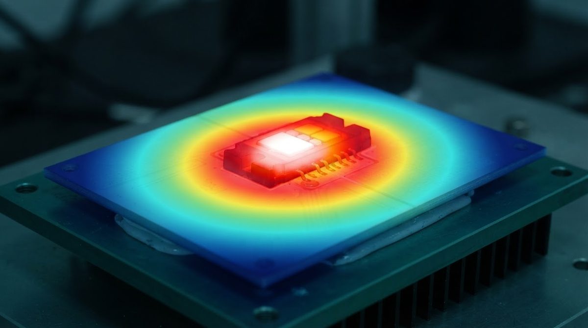
- Power modules (IGBT, SiC MOSFET): Aluminum nitride AlN thick film ceramic substrates serve as baseplates or direct die-attach carriers in modules rated 600 V and above.
- High-power LED and UV-C LED starboards: AlN spreads heat from high-flux LED arrays where alumina would create a thermal bottleneck.
- RF power amplifiers: The combination of low dielectric loss and high thermal conductivity suits GaN-on-SiC PA packages.
- Sensor packages: CTE-matched AlN carriers for silicon MEMS sensors reduce thermomechanical stress during reflow.
When Not to Use AlN Thick Film
If your device dissipates under 5 W per cm² and junction temperature is not the binding constraint, 96% alumina thick film will perform adequately at one-third to one-fifth the substrate cost. For applications requiring extreme mechanical toughness and thermal cycling beyond 3 000 power cycles (ΔT > 150 °C), Si₃N₄ AMB substrates offer superior fracture toughness (6–7 MPa·m^½ vs. 2.5–3.5 for AlN) at higher cost. For sub-25 µm features, switch from thick film to thin film deposition. And if your circuit needs plated through-holes and multi-layer routing, an LTCC or standard PCB stackup is a better architecture than thick film on a monolithic ceramic.
FAQ
Can you solder directly to AlN thick film metallization?
Yes, provided the thick film conductor is topped with a solderable finish such as electroless nickel / immersion gold (ENIG) or plated Ni/Au. Bare fired silver is solderable with SnAgCu pastes, but wettability degrades after storage. A nickel barrier layer also prevents silver leaching into the solder joint.
Does AlN degrade in humidity?
Unprotected AlN slowly hydrolyzes in hot, humid environments, forming aluminum hydroxide on the surface. At 85 °C / 85% RH, measurable surface degradation can appear within 500 hours on unmetallized areas. Metallization and conformal coating effectively block moisture access. Design exposed AlN edges out of condensation zones or seal them.
What atmosphere is needed to fire thick film pastes on AlN?
Nitrogen with oxygen content below 10 ppm is standard. Firing in air above 700 °C oxidizes the AlN surface, weakening paste adhesion and forming a thermally resistive alumina interlayer. Gold pastes are more tolerant of residual oxygen than silver pastes, but nitrogen firing is recommended for both.
How does AlN thick film cost compare to DBC on AlN?
AlN thick film substrates are typically 30–50% less expensive than AlN DBC (direct bonded copper) for equivalent substrate sizes, because thick film avoids the high-temperature copper bonding step. However, DBC provides much thicker copper (0.2–0.3 mm) for higher current carrying capacity. Choose thick film for signal-level and moderate-current circuits; choose DBC when copper thickness above 50 µm is required.
What is the maximum continuous operating temperature for an aluminum nitride AlN thick film ceramic assembly?
The AlN ceramic itself is stable to 1 000 °C in inert atmosphere. The practical limit is set by the metallization: fired silver conductors are rated to roughly 300 °C, while gold conductors can operate to 500 °C. Solder joints (SnAgCu) limit most assemblies to 150–200 °C. Sintered silver die attach extends the assembly limit to about 300 °C.
Next Step
If AlN thick film fits your thermal and electrical requirements, request a ceramic substrate sample kit to verify paste adhesion and solderability with your own assembly process before committing to production volumes.