Standard ceramic substrates ship in thicknesses from 0.25 mm to 1.0 mm, with 0.38 mm and 0.635 mm accounting for the majority of production volume. Thinner substrates lower thermal resistance but reduce mechanical strength; thicker ones survive handling and thermal cycling better but add thermal impedance. The chart below gives you the numbers to make that trade-off for Al₂O₃ (96% and 99.6%), AlN, and Si₃N₄.
Standard Ceramic Substrate Thickness Chart
| Nominal Thickness (mm) | Nominal Thickness (in) | Typical Tolerance | Common Materials | Primary Use Cases |
|---|---|---|---|---|
| 0.25 | 0.010 | ±0.025 mm | Al₂O₃ 96%, AlN | High-density thin-film circuits, RF hybrids |
| 0.32 | 0.013 | ±0.025 mm | Al₂O₃ 96%, AlN | LED submounts, compact power modules |
| 0.38 | 0.015 | ±0.03 mm | Al₂O₃ 96%, AlN, Si₃N₄ | Power electronics, DBC/AMB substrates |
| 0.50 | 0.020 | ±0.03 mm | Al₂O₃ 96%/99.6%, AlN | General thick-film circuits, sensor substrates |
| 0.635 | 0.025 | ±0.05 mm | Al₂O₃ 96%/99.6%, AlN, Si₃N₄ | Industry-standard thickness for most hybrid circuits |
| 0.80 | 0.031 | ±0.05 mm | Al₂O₃ 96% | Higher-voltage isolation, structural substrates |
| 1.0 | 0.040 | ±0.05 mm | Al₂O₃ 96%/99.6%, AlN | High-voltage isolation (>5 kV), mechanical carriers |
Typical values for commercially available material, for comparison only. Confirm against the datasheet for your specific grade. Tolerances per Kyocera and CoorsTek published substrate specifications.
The 0.635 mm (25 mil) thickness is the de facto standard inherited from decades of thick-film hybrid production. If your design has no strong reason to deviate, start there. It balances thermal performance, dielectric strength, flatness, and ease of handling during metallization and assembly.
How Thickness Affects Thermal Resistance

Substrate thermal resistance scales linearly with thickness and inversely with thermal conductivity and area. The one-dimensional approximation is:
Rth = t / (k × A)
where t is thickness (m), k is thermal conductivity (W/m·K), and A is the heat-transfer area (m²). For a detailed comparison of k values across materials, see the thermal conductivity table for ceramic PCB materials.
Worked Example: 96% Al₂O₃, 10 × 10 mm Footprint
| Thickness (mm) | Rth (°C/W) | ΔT at 5 W (°C) |
|---|---|---|
| 0.25 | 1.0 | 5.0 |
| 0.38 | 1.52 | 7.6 |
| 0.635 | 2.54 | 12.7 |
| 1.0 | 4.0 | 20.0 |
Calculated using k = 25 W/m·K (mid-range for 96% Al₂O₃ at 25 °C) and A = 100 mm². Real spreading resistance will be higher; use FEA for production designs.
Going from 0.635 mm to 0.38 mm cuts thermal resistance by 40%. For a power die dissipating 5 W through a 10 × 10 mm footprint, that is a 5.1 °C reduction in temperature drop across the substrate alone. In LED and IGBT applications, that margin often determines whether you can stay within Tj,max without a larger heat spreader. For layouts that rely on the substrate itself as a spreader, the ceramic heat spreader design guide covers geometry and copper-layer strategies in detail.
AlN substrates (170–200 W/m·K at 25 °C, per CoorsTek ADS-995 and Maruwa datasheets) are far less sensitive to thickness changes. At 0.635 mm on the same 10 × 10 mm area, Rth drops to roughly 0.35 °C/W. If you are already using AlN, going thinner for thermal reasons alone rarely justifies the added fragility.
Mechanical Strength vs. Thickness
Ceramics fail by brittle fracture, not yield. Flexural strength (measured per ASTM C1161 three-point bend) does not change with thickness, but the load a substrate can survive before fracturing does. Bending stress in a simply supported plate scales as:
σ = 3FL / (2bt²)
Halving thickness from 0.635 mm to 0.32 mm quadruples the stress at a given load. In practice, substrates thinner than 0.38 mm require careful handling fixtures during screen printing, pick-and-place, and reflow. Automated assembly lines with vacuum nesting handle 0.25 mm routinely, but manual prototyping at that thickness invites breakage.
Si₃N₄ stands apart here. Its flexural strength (600–900 MPa, per Kyocera SN series datasheets) is roughly three times that of 96% Al₂O₃ (300–350 MPa) and AlN (300–350 MPa). That makes 0.32 mm Si₃N₄ mechanically comparable to 0.635 mm alumina under bending loads. Power module designers increasingly specify 0.32 mm Si₃N₄ AMB substrates to cut thermal resistance without sacrificing thermal cycling reliability.
Dielectric Strength and Voltage Isolation
Dielectric breakdown voltage scales roughly linearly with thickness for a given material. 96% Al₂O₃ breaks down at approximately 10–15 kV/mm (per CeramTec data). A 0.635 mm substrate therefore withstands 6.3–9.5 kV in a DC hipot test. For designs requiring >10 kV isolation, 1.0 mm is the standard choice.
AlN has a lower dielectric strength (14–17 kV/mm), but because its thermal conductivity is so much higher, you can use a thicker substrate without paying a large thermal penalty. A 1.0 mm AlN substrate still has lower thermal resistance than 0.635 mm alumina on the same footprint.
Flatness and Warpage at Different Thicknesses
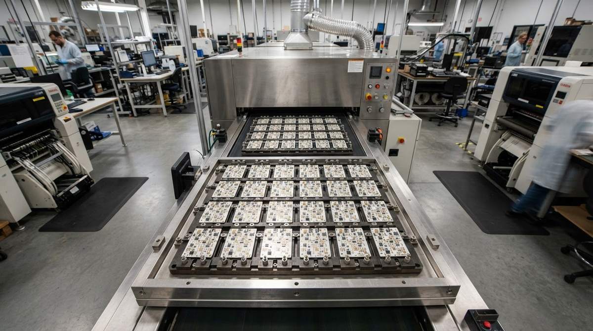
Thinner substrates warp more easily during metallization firing and solder reflow. As-fired camber for 96% Al₂O₃ is typically ≤0.1 mm per 25 mm of length at 0.635 mm thickness. At 0.25 mm, camber can reach 0.15–0.2 mm per 25 mm unless the substrate is lapped or constrained during processing. If your assembly process is sensitive to co-planarity, controlling ceramic substrate warpage and flatness becomes a critical step. Lapped-and-polished substrates add cost but hold flatness below 0.05 mm per 25 mm even at 0.25 mm thickness.
When Not to Use a Thin Ceramic Substrate
Thinner is not always better. Choose a thicker substrate or a different technology when:
- High-voltage isolation is the primary requirement. If you need >5 kV working voltage, 0.635 mm or 1.0 mm is safer. Thinning to 0.38 mm for thermal gain may force you into AlN cost territory just to maintain isolation margin.
- Manual handling dominates your assembly process. Substrates below 0.38 mm break easily without vacuum fixtures. If your line is not equipped for thin ceramics, yield loss will erase any thermal benefit.
- FR-4 or metal-core PCB meets your thermal budget. If your device dissipates under 1 W and operates below 130 °C, ceramic is likely over-specified. An aluminum-core MCPCB at 1.5 mm gives adequate thermal performance at a fraction of the cost.
- Large panel sizes are needed. Thin ceramic substrates above ~50 × 50 mm become difficult to keep flat through processing. If your design exceeds that footprint, consider tiling smaller substrates onto a metal baseplate.
Choosing the Right Thickness: A Decision Path
- Set your thermal budget. Calculate Rth,substrate at your target thickness using the formula above. If the temperature drop across the substrate is less than 10% of your total thermal budget, thickness is not your bottleneck—focus elsewhere.
- Check your isolation voltage. Divide the required withstand voltage by the material’s dielectric strength. Add a 50% safety margin. That gives you the minimum thickness.
- Verify mechanical survival. If the substrate will be handled manually or soldered without fixture support, stay at 0.38 mm or above for alumina and AlN. Si₃N₄ can go thinner.
- Confirm availability. Non-standard thicknesses (e.g., 0.40 mm, 0.75 mm) require custom firing runs and longer lead times. The seven thicknesses in the chart above are stocked by most suppliers.
For substrates that need copper plating on ceramic, note that plated copper thickness (typically 10–300 µm) adds to the total stackup height but does not contribute to dielectric isolation. Account for this in your mechanical envelope.
Frequently Asked Questions
Can I get a ceramic substrate thinner than 0.25 mm?
Yes. Some suppliers offer 0.15 mm and even 0.10 mm alumina and AlN substrates, typically for MEMS and thin-film RF applications. These require specialized handling and are not stocked—expect custom lead times of 6–10 weeks and higher per-unit cost.
Does substrate thickness affect copper adhesion?
Thickness itself does not change adhesion strength. However, thinner substrates are more prone to warpage during firing, which can cause localized delamination at copper-ceramic interfaces. Proper fixturing during metallization eliminates this risk.
Is 0.635 mm always the safest default?
For thick-film hybrid circuits operating below 2 kV with moderate power dissipation, 0.635 mm is a reliable default. Power modules with high current density often benefit from 0.38 mm or 0.32 mm to reduce thermal resistance. There is no universal “safest” choice—it depends on your thermal, electrical, and mechanical constraints.
How does substrate thickness affect cost?
Thinner substrates use less raw material but are harder to process and handle, so cost does not drop linearly. The sweet spot for cost is 0.50–0.635 mm. Going below 0.38 mm or above 1.0 mm typically adds 10–25% to substrate cost due to lower yields or extra material.
Do I need lapping for thin substrates?
As-fired substrates at 0.25–0.32 mm often meet ±0.025 mm thickness tolerance. If your application requires tighter tolerance (e.g., ±0.01 mm for die-attach co-planarity), lapping is necessary. Lapping adds cost but also improves surface finish, which benefits thin-film metallization adhesion.