An alumina 96% Al2O3 DPC direct plated copper substrate is a ceramic circuit board where copper is deposited directly onto a 96%-purity alumina base using sputtering and electroplating, then patterned by photolithography and etching. The result is a metallized ceramic with trace/space resolution down to 30–50 µm, thermal conductivity of 24–28 W/mK (at 25 °C, per Kyocera and CoorsTek datasheets), and copper adhesion strength typically above 6 N/mm — all at a lower substrate cost than 99.6% alumina or aluminum nitride alternatives. For engineers evaluating alumina 96% Al2O3 DPC direct plated copper for power, LED, or RF modules, this page covers the process, properties, trade-offs, and design rules you need.
Key Takeaways
- DPC on 96% alumina achieves 30–50 µm line/space, finer than thick film (~100 µm) and comparable to thin film on the same substrate.
- Thermal conductivity of 96% Al2O3 ranges from 24–28 W/mK at 25 °C, roughly 6–7× that of FR-4 (0.3–0.4 W/mK).
- Copper thickness is adjustable from roughly 5 µm to 100+ µm via electroplating, giving designers flexibility for high-current or fine-pitch layouts on a single substrate.
- The CTE of 96% alumina (6.5–7.2 ppm/°C, 25–300 °C, per CoorsTek ADS-96R datasheet) is a close match to GaAs and SiC die, reducing solder-joint fatigue in power and RF modules.
- 96% alumina DPC is the cost-effective entry point for ceramic DPC; step up to 99.6% Al2O3 DPC ceramic substrates only when you need higher purity for lower dielectric loss or tighter mechanical tolerances.
How the Alumina 96% Al2O3 DPC Direct Plated Copper Process Works
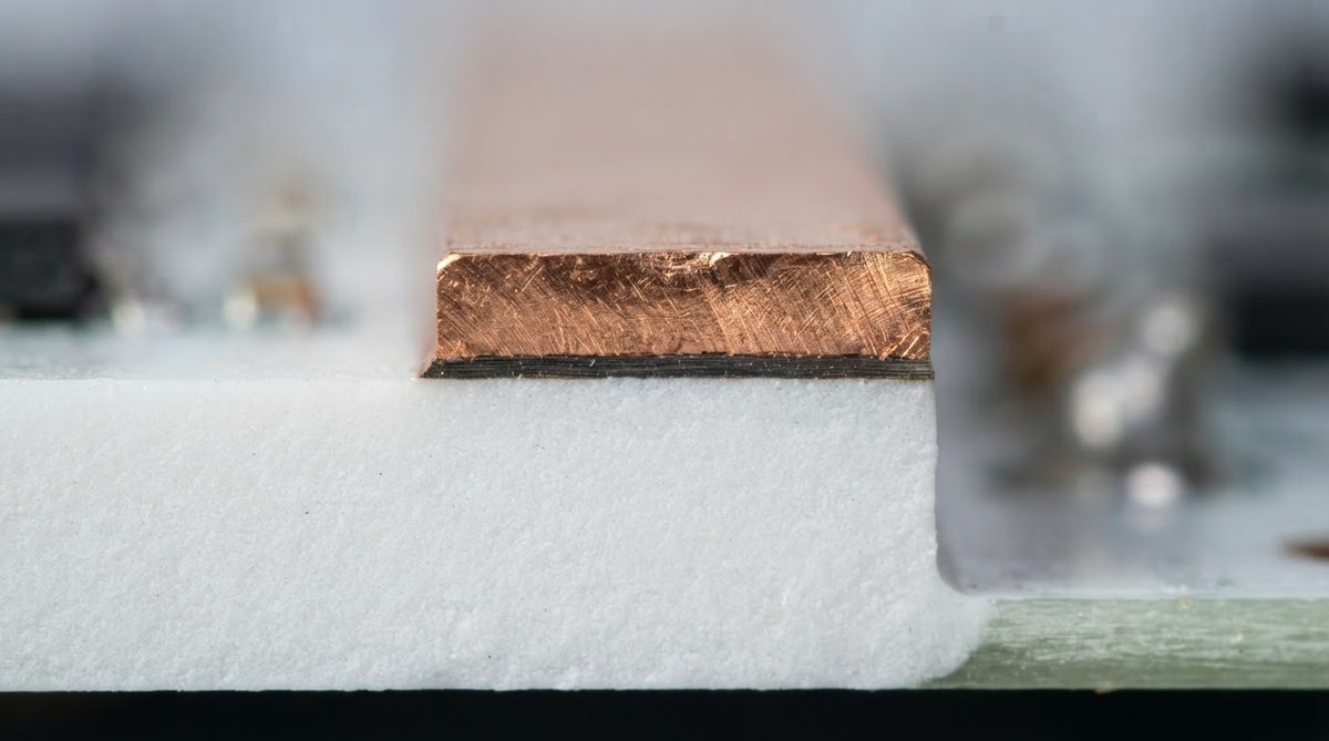
DPC — direct plated copper — is a subtractive metallization method. The process begins with a polished 96% Al2O3 substrate, typically 0.25–1.0 mm thick. A thin adhesion layer (commonly titanium or chromium, 20–50 nm) is sputtered onto the ceramic surface, followed by a copper seed layer (200–500 nm). Copper is then electroplated to the target thickness. Finally, photoresist is applied, the circuit pattern is exposed and developed, and unwanted copper is etched away.
This sequence produces several advantages over screen-printed thick film conductors. Because the copper is plated rather than printed, the conductor is pure Cu with bulk resistivity near 1.7 µΩ·cm — roughly 5–10× lower than the silver or gold pastes used in alumina 96% thick film substrates. The photolithographic patterning also delivers much finer features than screen printing, which is limited by mesh count and paste rheology.
Material Properties: Alumina 96% Al2O3 DPC Substrate Specifications
| Parameter | Value | Unit | Condition | Source |
|---|---|---|---|---|
| Thermal conductivity | 24–28 | W/mK | 25 °C | CoorsTek ADS-96R / Kyocera A-493 |
| Dielectric constant (εr) | 9.0–9.5 | — | 1 MHz, 25 °C | CoorsTek ADS-96R |
| Dielectric strength | 14–17 | kV/mm | AC, 25 °C | CoorsTek ADS-96R |
| CTE | 6.5–7.2 | ppm/°C | 25–300 °C | CoorsTek ADS-96R |
| Flexural strength | 340–380 | MPa | ASTM C1161, 4-pt bend | CoorsTek ADS-96R |
| Surface roughness (Ra) | 0.3–0.6 | µm | As-fired, polished face | Typical commercial grade |
| Cu thickness (DPC) | 5–100+ | µm | Electroplated | Process-dependent |
| Min trace/space (DPC) | 30–50 | µm | Photolithography | Process-dependent |
| Cu adhesion (peel strength) | > 6 | N/mm | IPC-TM-650 2.4.8 | Typical for sputtered Ti/Cu on Al2O3 |
Typical values for commercially available material, for comparison only. Confirm against the datasheet for your specific grade.
DPC vs. Thick Film vs. Thin Film on 96% Alumina
All three metallization methods use the same 96% Al2O3 base. The differences are in conductor material, resolution, and cost. Choosing alumina 96% Al2O3 DPC direct plated copper gives you a middle path between thick film economy and thin film precision.
| Feature | DPC | Thick Film | Thin Film |
|---|---|---|---|
| Conductor | Pure Cu (electroplated) | Ag, Au, or AgPd paste | Sputtered NiCr/Au or Ti/Cu |
| Min line/space | 30–50 µm | ~100 µm | 10–25 µm |
| Conductor resistivity | ~1.7 µΩ·cm | 2–5 µΩ·cm (Ag paste) | ~1.7 µΩ·cm (Cu) / ~2.2 µΩ·cm (Au) |
| Max Cu thickness | 100+ µm | 10–25 µm (paste) | 1–5 µm typical |
| Best for | Power, LED, medium RF | Resistor networks, hybrid ICs | Precision RF, mmWave |
| Relative cost | Medium | Low | High |
DPC occupies the middle ground. It gives you finer lines than thick film and thicker copper than thin film. If your design needs embedded resistors, thick film is the natural choice. If you need sub-25 µm features for millimeter-wave circuits, consider alumina 96% thin film substrates instead.
Worked Example: Thermal Resistance of an Alumina 96% DPC Power Substrate
Suppose you mount a 10 W laser diode on a 96% Al2O3 DPC substrate, 0.635 mm thick, with a heat-spreading footprint of 5 mm × 5 mm.
Thermal resistance through the ceramic: Rth = t / (k × A) = 0.000635 m / (26 W/mK × 0.000025 m²) = 0.98 °C/W.
At 10 W dissipation, the temperature rise across the substrate alone is about 9.8 °C. If that delta is too large, your options are: reduce thickness to 0.38 mm (Rth drops to ~0.58 °C/W), increase the spreading area, or move to aluminum nitride DPC substrates where k = 170–200 W/mK cuts Rth by roughly 7×.
Enter your substrate dimensions, material, and power dissipation below to calculate thermal resistance for your own alumina 96% Al2O3 DPC direct plated copper layout or any alternative ceramic substrate.
Typical Applications for Alumina 96% Al2O3 DPC Direct Plated Copper
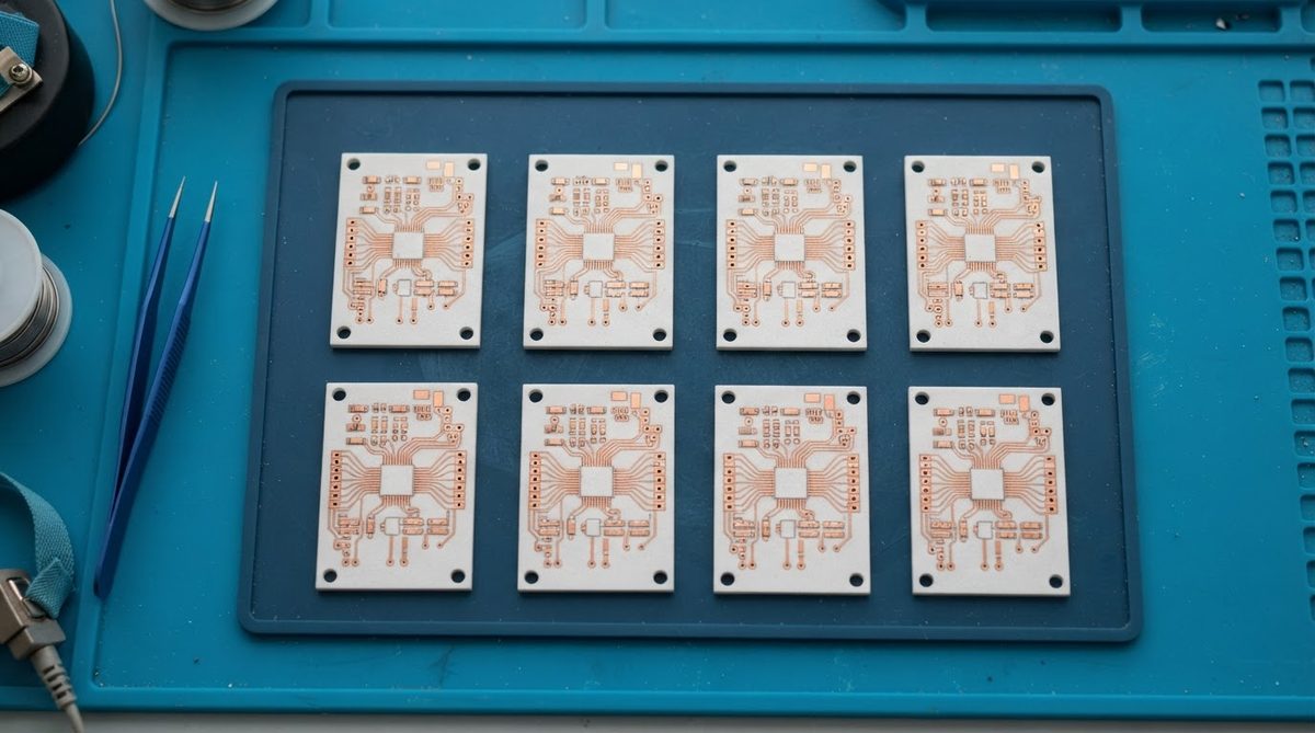
96% alumina DPC substrates appear most often in high-brightness LED modules, power semiconductor packages (IGBT, MOSFET die attach), RF hybrid assemblies up to a few GHz, sensor modules, and automotive LIDAR driver boards. The combination of decent thermal conductivity, high electrical isolation, and fine copper patterning makes it a practical choice wherever FR-4 or metal-core PCBs cannot meet thermal or reliability requirements.
When Not to Use 96% Alumina DPC
If your power density is extreme — above roughly 100 W/cm² at the die — 96% alumina’s 24–28 W/mK may not keep junction temperatures safe. AlN DPC or Si3N4 AMB substrates are better suited. For silicon nitride AMB ceramic substrates, the mechanical toughness also handles severe thermal cycling that would crack alumina.
If your circuit runs above 20 GHz and requires ultra-low loss tangent (tan δ < 0.001), 99.6% alumina or sapphire will outperform 96% alumina, whose glassy grain-boundary phase increases dielectric loss at high frequencies.
If your BOM target is under $0.50 per board and thermal demands are modest, FR-4 or aluminum MCPCB will cost a fraction of any ceramic solution. Ceramic substrates make economic sense only when the performance gap justifies the price difference.
Design Tips for Alumina 96% Al2O3 DPC Layouts
- Match CTE to die. 96% alumina’s 6.5–7.2 ppm/°C pairs well with SiC (4.0 ppm/°C) and GaAs (5.7 ppm/°C) using AuSn or SAC solder. For large die (> 10 mm), run a solder-fatigue simulation.
- Specify substrate thickness early. Standard options are 0.25, 0.38, 0.50, 0.635, and 1.0 mm. Check the ceramic substrate thickness chart before committing a stackup.
- Mind copper stress. Thick copper (> 70 µm) on thin ceramic (< 0.38 mm) can warp or crack the substrate during thermal cycling. Balance copper thickness on both sides, or use a back-side ground plane of similar thickness.
- Surface finish. DPC copper can be finished with ENIG, ENEPIG, OSP, or bare Au plating depending on the assembly method. Specify the finish at quoting stage to avoid re-work.
Frequently Asked Questions
Can I get vias in a 96% alumina DPC substrate?
Yes. Vias are laser-drilled or mechanically punched before metallization, then plated with copper during the DPC process. Minimum via diameter is typically 100–200 µm depending on substrate thickness. Through-vias are standard; blind vias are possible but add cost.
How does DPC copper adhesion compare to DBC?
DPC peel strength is typically above 6 N/mm (per IPC-TM-650 2.4.8), while DBC (direct bond copper) achieves 8–12 N/mm because the oxide bonding layer creates a stronger interface. For most applications below 200 A/cm², DPC adhesion is more than adequate.
Is 96% alumina DPC suitable for automotive under-hood environments?
It handles continuous operating temperatures up to 300 °C and passes thermal shock testing from −55 °C to +150 °C (per MIL-STD-883 Method 1010). Many automotive LIDAR and power modules use this substrate. Confirm your specific cycling profile with the manufacturer.
What is the typical lead time for prototype alumina 96% Al2O3 DPC direct plated copper substrates?
Prototype quantities (5–25 pieces) generally ship in 2–4 weeks depending on complexity and surface finish. Production runs with established tooling are faster. Request a quote with your Gerber files to get an exact timeline.
Does DPC work on substrates thinner than 0.25 mm?
It is possible but risky. Substrates below 0.25 mm are fragile during handling and prone to cracking under copper stress. Most manufacturers set 0.25 mm as the practical minimum for DPC. Thin film metallization is more forgiving at these thicknesses because the metal layer is much thinner.
Next Step
If alumina 96% Al2O3 DPC direct plated copper fits your thermal and resolution requirements, prepare your Gerber or DXF files and submit them through our instant quote page for pricing and lead time. For projects needing higher thermal conductivity, review the aluminum nitride DPC option to compare costs side by side.