A sapphire substrate is a single-crystal form of aluminum oxide (α-Al₂O₃, 99.99 %+ purity) grown by methods such as Czochralski, Kyropoulos, or edge-defined film-fed growth (EFG). It offers a combination of high optical transparency (from deep UV to mid-IR), excellent surface finish (Ra < 0.3 nm after CMP), and thermal conductivity of 35–46 W/m·K at 25 °C—roughly 40–60 % higher than 96 % polycrystalline alumina. These properties make sapphire the substrate of choice for GaN-on-sapphire LEDs, UV-C emitters, RF MEMS, and high-temperature sensor windows, but its cost and processing constraints mean it is not the right pick for every ceramic PCB application.
Key Takeaways
- Sapphire thermal conductivity is 35–46 W/m·K at 25 °C (per Kyocera and CoorsTek datasheets), compared with 24–28 W/m·K for 96 % alumina and 170–200 W/m·K for aluminum nitride.
- Optical transmission extends from approximately 150 nm (deep UV) to about 5.5 µm (mid-IR), making sapphire transparent across the full UV-C band (200–280 nm).
- Mohs hardness of 9 means sapphire resists scratching and chemical attack but is difficult and expensive to machine after growth.
- Lattice mismatch with GaN is about 16 %, which is managed through buffer layers in LED and RF epitaxy but still limits defect density compared with native GaN substrates.
- Cost per unit area is typically 5–15× that of 96 % polycrystalline alumina, depending on diameter, orientation, and surface specification.
What Is a Sapphire Substrate?
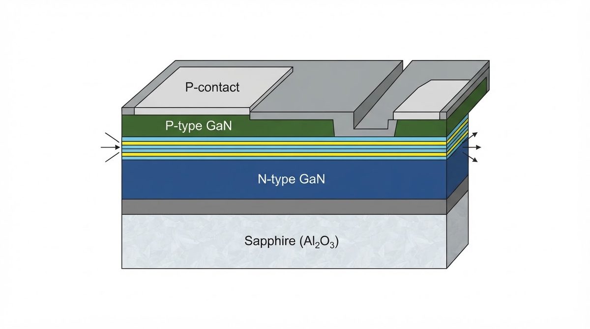
Sapphire substrates are wafers sliced from boules of single-crystal corundum. Because the crystal is grown from a melt of high-purity alumina feedstock, the resulting material contains no grain boundaries, pores, or secondary phases. This gives sapphire its defining advantages over polycrystalline 96 % alumina ceramic: near-theoretical density (3.98 g/cm³), uniform dielectric behavior across the surface, and optical clarity from the deep ultraviolet through the mid-infrared.
Standard orientations include C-plane (0001), R-plane (1-102), A-plane (11-20), and M-plane (10-10). The choice of crystal orientation affects lattice matching to epitaxial films, thermal expansion behavior, and optical axis alignment. C-plane is by far the most common for LED and electronic applications.
Key Material Properties of Sapphire
| Parameter | Value | Unit | Condition | Source |
|---|---|---|---|---|
| Crystal structure | Hexagonal (corundum) | — | — | Kyocera datasheet |
| Purity | ≥ 99.99 | % | — | CoorsTek / Kyocera |
| Density | 3.97–3.98 | g/cm³ | 25 °C | CoorsTek |
| Thermal conductivity (C-axis) | 42–46 | W/m·K | 25 °C | Kyocera |
| Thermal conductivity (A-axis) | 35–40 | W/m·K | 25 °C | Kyocera |
| CTE (C-axis) | 5.0 | ppm/°C | 20–200 °C | CoorsTek |
| CTE (A-axis) | 5.6 | ppm/°C | 20–200 °C | CoorsTek |
| Dielectric constant (εr) | 9.4 (C-axis) / 11.6 (A-axis) | — | 1 MHz, 25 °C | Kyocera |
| Dielectric strength | 40–48 | kV/mm | 25 °C, DC | CoorsTek |
| Flexural strength | 350–690 | MPa | 25 °C, 3-pt bend | CoorsTek |
| Mohs hardness | 9 | — | — | — |
| Optical transmission range | ~150–5500 | nm | > 80 % T, 1 mm thick | Kyocera |
| Max use temperature | ~1800 | °C | Inert atmosphere | CoorsTek |
Typical values for commercially available material, for comparison only. Confirm against the datasheet for your specific grade.
Two properties stand out for electronic designers. First, the anisotropic dielectric constant: εr varies from 9.4 to 11.6 depending on crystal axis orientation relative to the electric field, which matters for RF impedance calculations. Second, sapphire’s CTE of 5.0–5.6 ppm/°C sits between silicon (2.6 ppm/°C) and GaN (5.6 ppm/°C on A-axis), giving it a reasonable thermal expansion match to GaN epilayers.
Sapphire vs. Polycrystalline Alumina vs. Quartz
Engineers evaluating sapphire often compare it against standard alumina ceramics and quartz (SiO₂) substrates. The table below puts the three side by side.
| Parameter | Sapphire (single-crystal Al₂O₃) | 96 % Alumina (polycrystalline) | Fused Quartz (SiO₂) |
|---|---|---|---|
| Thermal conductivity (25 °C) | 35–46 W/m·K | 24–28 W/m·K | 1.3–1.5 W/m·K |
| CTE (20–200 °C) | 5.0–5.6 ppm/°C | 6.5–7.2 ppm/°C | 0.5–0.6 ppm/°C |
| Dielectric constant (1 MHz) | 9.4–11.6 | 9.0–9.5 | 3.7–3.8 |
| UV transparency (250 nm) | > 80 % (1 mm) | Opaque | > 80 % (1 mm) |
| Surface roughness (polished) | < 0.3 nm Ra | ~0.1–0.5 µm Ra (lapped) | < 0.5 nm Ra |
| Relative cost (per cm²) | 5–15× | 1× (baseline) | 2–5× |
Sources: Kyocera, CoorsTek, and Heraeus datasheets. Cost multipliers are approximate market ratios for 2-inch substrates.
Sapphire wins on thermal conductivity and UV transparency simultaneously. Quartz transmits UV well but conducts heat poorly. Polycrystalline alumina conducts heat adequately but is opaque. If your design needs both thermal spreading and optical access, sapphire is the only single-material answer.
Common Electronic Applications
GaN-on-Sapphire LEDs and UV-C Emitters
More than 80 % of commercial GaN LEDs are grown on C-plane sapphire. The 16 % lattice mismatch is large, but decades of buffer-layer engineering (typically AlN or low-temperature GaN nucleation layers) have made the process reliable and cost-effective. For UV-C emitters operating at 260–280 nm, sapphire’s transparency below 300 nm is essential; the substrate also serves as the optical window. Designers working on UV-C LED starboards often mount these sapphire-based die onto AlN or alumina carrier PCBs for thermal management.
RF and MEMS Devices
Sapphire’s low dielectric loss tangent (tan δ ≈ 1 × 10⁻⁵ at 10 GHz, per Kyocera) and chemical stability make it attractive for thin-film RF filters, resonators, and MEMS pressure sensors. The atomically smooth surface enables deposition of high-quality piezoelectric films (AlN, ScAlN) with minimal interfacial defects.
High-Temperature Sensors and Windows
Sapphire retains mechanical integrity above 1 000 °C and remains optically transparent at elevated temperatures. Pyrometer windows, optical viewports in combustion chambers, and high-temperature pressure transducers commonly use sapphire substrates.
Worked Example: Thermal Resistance Through a Sapphire Window
Suppose you have a 10 mm × 10 mm sapphire window, 0.5 mm thick, conducting 2 W of heat from an LED die to a heat sink. The one-dimensional conduction resistance is:
Rth = t / (k × A)
Where t = 0.5 × 10⁻³ m, k = 42 W/m·K (C-axis), and A = 1 × 10⁻⁴ m².
Rth = 0.0005 / (42 × 0.0001) = 0.119 °C/W
At 2 W, the temperature drop across the sapphire is 0.24 °C. For comparison, the same geometry in fused quartz (k = 1.4 W/m·K) gives Rth = 3.57 °C/W and a 7.1 °C drop. The difference is small at 2 W but matters as power density increases or substrate area shrinks. If your design pushes above 10 W/cm², consider comparing sapphire against 99.6 % alumina (k ≈ 30–35 W/m·K) or AlN (k ≈ 170–200 W/m·K) depending on whether optical transparency is required.
Processing and Metallization Considerations
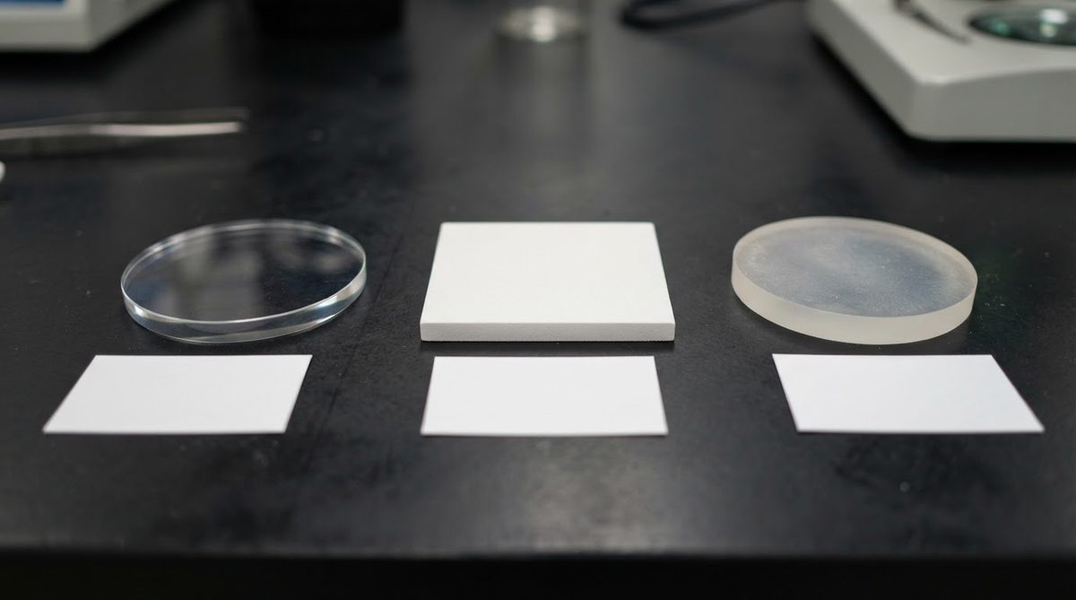
Sapphire cannot be processed like polycrystalline alumina. It is not fired from a green tape, so HTCC and LTCC processes do not apply. Substrates are sliced from boules using wire saws or ID saws, then lapped and polished. Typical epi-ready polish specifications call for Ra < 0.3 nm and total thickness variation (TTV) < 3 µm across a 2-inch wafer.
Metallization is done by thin-film sputtering or evaporation (Ti/Pt/Au, Cr/Au, Ti/Al stacks), not thick-film screen printing. The atomically smooth surface gives excellent adhesion with proper seed layers but does not accept conventional thick-film pastes well. For projects requiring patterned metallization on alumina, metallized ceramic substrates using polycrystalline alumina with thick-film or DPC processes are far more practical and cost-effective.
Sapphire Substrate Sizes and Thickness
Sapphire wafers are produced in standard semiconductor diameters: 2-inch (50.8 mm), 3-inch, 4-inch (100 mm), and 6-inch (150 mm). Larger diameters are available but at steep cost premiums. Thickness typically ranges from 0.1 mm to 1.0 mm for electronic substrates, with 0.43 mm and 0.65 mm being common for LED epi wafers. For reference on ceramic substrate sizing in general, see standard ceramic substrate sizes.
When NOT to Use Sapphire
Cost-sensitive designs. If your application does not require optical transparency or an atomically smooth surface, polycrystalline 96 % or 99.6 % alumina delivers adequate thermal and dielectric performance at a fraction of the cost. A thermal design guide for alumina PCBs can help you evaluate whether standard alumina meets your thermal budget.
High thermal conductivity without optical needs. Aluminum nitride substrates offer 170–200 W/m·K, roughly 4–5× sapphire’s conductivity. If your sole driver is heat spreading and you do not need UV transparency, AlN is the better material.
Complex multilayer circuits. Sapphire is a single-layer substrate. You cannot build vias, internal planes, or multilayer stackups in it. For multilayer ceramic circuits, HTCC or LTCC using polycrystalline alumina or glass-ceramic tapes is the standard approach.
Large-area boards. Sapphire wafers max out around 150 mm (6-inch) diameter at reasonable cost. If your board exceeds that, polycrystalline alumina panels up to 190 mm × 190 mm or larger are readily available.
Frequently Asked Questions
Is sapphire the same material as alumina?
Sapphire is single-crystal aluminum oxide (α-Al₂O₃) at 99.99 %+ purity. Standard alumina substrates are polycrystalline, typically 96 % or 99.6 % Al₂O₃ with glass-phase binders. The chemical formula is the same, but the crystal structure, purity, optical behavior, and cost are very different.
Can you solder components directly to a sapphire substrate?
Yes, but only after depositing a thin-film metallization stack (commonly Ti/Pt/Au or Ti/Ni/Au) by sputtering or evaporation. Bare sapphire is not wettable by solder. The metallization must be patterned lithographically, which adds cost compared with screen-printed thick-film on standard alumina.
What is the maximum operating temperature of sapphire?
Sapphire retains structural integrity up to approximately 1 800 °C in inert atmosphere and roughly 1 600 °C in air before surface degradation becomes significant. Metallization layers will fail well before the sapphire itself, so the practical limit depends on your metal stack and solder alloy.
Does sapphire work for RF applications above 10 GHz?
Sapphire performs well at microwave and millimeter-wave frequencies due to its low loss tangent (tan δ ≈ 1 × 10⁻⁵ at 10 GHz). The anisotropic dielectric constant (9.4–11.6 depending on orientation) must be accounted for in impedance calculations. For lower-cost RF substrates where optical transparency is unnecessary, polycrystalline alumina or quartz may suffice.
How thin can a sapphire substrate be made?
Production sapphire wafers are routinely thinned to 100 µm (0.1 mm) by lapping and CMP. Thinner substrates down to 50 µm are possible but fragile and expensive. For LED applications, laser lift-off processes can remove the sapphire entirely after GaN growth.
Next Step
If your project requires a ceramic substrate but sapphire’s cost or single-crystal constraints are a concern, polycrystalline alumina or AlN may be the better fit. Compare material options and request pricing through the AluminaPCB custom substrate page.