What Is an Alumina 99.6% Al2O3 Thin Film Ceramic Substrate?
An alumina 99.6% Al2O3 thin film ceramic substrate is a high-purity aluminum oxide base plate engineered for sputtered or evaporated metallization at line/space resolutions down to 10 µm or finer. Compared to 96% alumina thin film substrates, the 99.6% grade delivers a smoother as-fired surface, tighter grain structure, and better high-frequency dielectric performance at a modest cost premium. This makes alumina 99.6% Al2O3 thin film ceramic the workhorse substrate for precision resistor networks, MEMS sensor packages, RF hybrid circuits, and medical implant electronics.
Key Properties of Alumina 99.6% Al2O3 Thin Film Ceramic
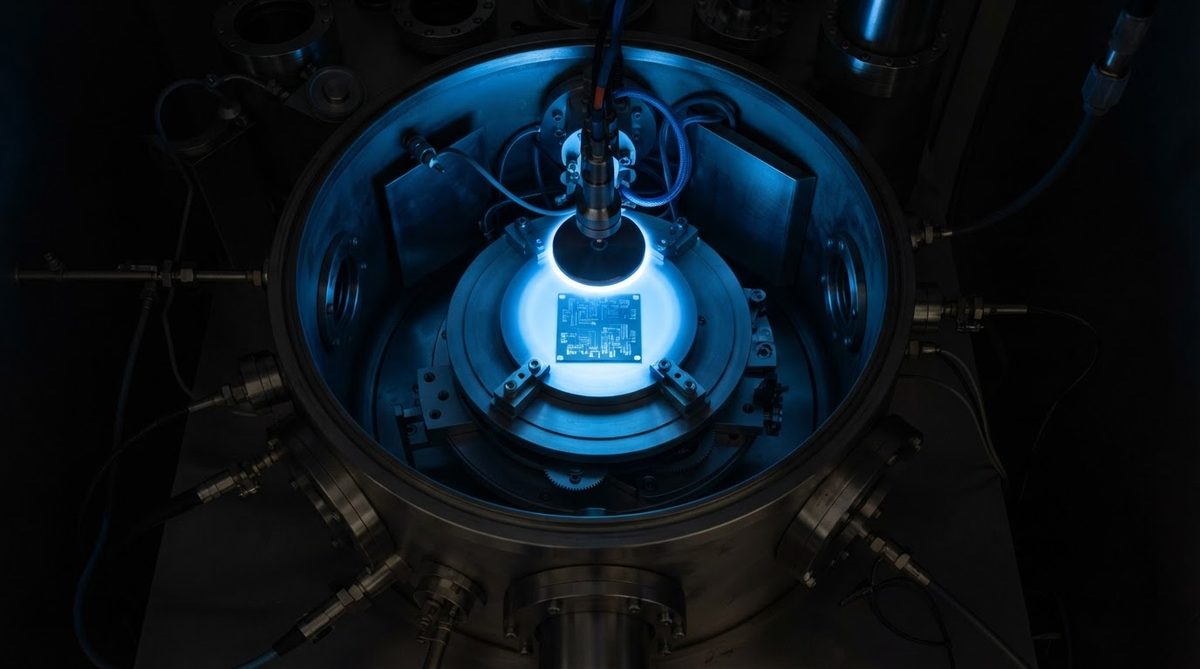
The table below summarises the properties that matter most for thin film circuit design. Values are for commercially available 99.6% alumina from major suppliers (Kyocera A-493, CoorsTek AD-996, Maruwa HA-996).
| Parameter | Value | Unit | Condition | Source |
|---|---|---|---|---|
| Al2O3 purity | ≥ 99.6 | % | — | Kyocera A-493 datasheet |
| Thermal conductivity | 28–35 | W/mK | 20 °C, ASTM E1461 | CoorsTek AD-996 datasheet |
| Dielectric constant (εr) | 9.7–9.9 | — | 1 MHz, 25 °C | Kyocera A-493 datasheet |
| Loss tangent (tan δ) | 0.0001–0.0003 | — | 1 MHz, 25 °C | Kyocera A-493 datasheet |
| Dielectric strength | 14–17 | kV/mm | AC, 60 Hz | CoorsTek AD-996 datasheet |
| Flexural strength | 400–450 | MPa | ASTM C1161, 4-pt bend | CoorsTek AD-996 datasheet |
| Surface roughness (Ra), lapped & polished | 0.02–0.05 | µm | Optical profilometry | Maruwa HA-996 datasheet |
| CTE | 7.2–7.9 | ppm/°C | 25–400 °C | Kyocera A-493 datasheet |
| Volume resistivity | ≥ 1014 | Ω·cm | 25 °C | CoorsTek AD-996 datasheet |
| Max continuous use temperature | 1 600 | °C | In air, unloaded | CoorsTek AD-996 datasheet |
Typical values for commercially available material, for comparison only. Confirm against the datasheet for your specific grade.
Why 99.6% Instead of 96% Alumina for Thin Film Circuits?
The 3.6-percentage-point purity jump matters more than it sounds. In 96% alumina, the remaining 4% is a silica-rich glass phase that fills grain boundaries. That glass phase limits three things thin film designers care about:
- Surface finish. As-fired 96% alumina typically measures Ra 0.3–0.8 µm. Even after lapping it rarely gets below Ra 0.1 µm without excessive material removal. The alumina 99.6% Al2O3 thin film ceramic grade fires with a finer, more uniform grain (1–3 µm average), reaching Ra < 0.05 µm after a standard lap-and-polish cycle. Sputtered TaN or NiCr thin film resistors need Ra < 0.1 µm to hold ±1% tolerance.
- Dielectric loss. The glass phase in 96% alumina raises tan δ to roughly 0.0005–0.001 at 1 MHz. At microwave frequencies the gap widens further. For RF hybrids above 5 GHz, the lower loss of 99.6% alumina (tan δ ≤ 0.0003) reduces insertion loss by a measurable margin.
- Outgassing. Glass-phase constituents can outgas during vacuum deposition, contaminating sputtering targets and degrading film adhesion. High-purity alumina outgasses far less, which improves first-pass yield in thin film processing.
The trade-off is cost. Expect 99.6% alumina blanks to run 1.5–2.5× the price of equivalent 96% blanks, depending on size and finish. For thick film circuits with 100 µm line/space, that premium buys nothing useful. For thin film circuits below 25 µm line/space, it pays for itself in yield.
Thin Film Process Compatibility
Thin film metallization on alumina 99.6% Al2O3 thin film ceramic substrates typically follows this sequence:
- Substrate preparation. Incoming blanks are ultrasonically cleaned, then inspected for surface defects. Any scratch deeper than 0.5 µm can cause an open in a 10 µm trace.
- Adhesion layer. A 20–50 nm layer of Ti or Cr is sputtered to promote bonding between the ceramic and the conductor.
- Conductor layer. Au, Cu, or Pt is sputtered or e-beam evaporated to the target thickness (typically 0.5–5 µm). For resistor networks, TaN or NiCr is deposited to a controlled sheet resistance.
- Photolithography. Resist is spun, exposed, and developed. The smooth substrate surface allows uniform resist thickness, which is critical for resolving features below 20 µm.
- Etching. Wet or ion-beam etching defines the circuit pattern.
- Passivation. SiO2 or Si3N4 dielectric is deposited over resistors for long-term stability.
The fine grain structure of 99.6% alumina keeps sputtered film stress uniform across the substrate, reducing micro-cracking in resistor layers after thermal cycling. This is why precision thin film resistor manufacturers (Vishay, International Manufacturing Services) specify 99.6% or higher purity.
How Alumina 99.6% Al2O3 Thin Film Ceramic Compares to AlN and Sapphire
When 99.6% alumina does not meet a thermal or optical requirement, engineers typically look at aluminum nitride or sapphire. The comparison below helps decide.
| Parameter | 99.6% Al2O3 | AlN | Sapphire |
|---|---|---|---|
| Thermal conductivity (W/mK) | 28–35 | 170–200 | 25–42 |
| εr at 1 MHz | 9.7–9.9 | 8.5–8.9 | 9.3–11.5 (anisotropic) |
| tan δ at 1 MHz | 0.0001–0.0003 | 0.0003–0.001 | < 0.0001 |
| CTE (ppm/°C, 25–400 °C) | 7.2–7.9 | 4.4–4.7 | 5.0–7.7 |
| Surface Ra, polished (µm) | 0.02–0.05 | 0.02–0.05 | < 0.005 |
| Relative substrate cost | 1× | 3–5× | 5–15× (size-dependent) |
| Optical transparency | Opaque | Opaque | Transparent (UV–IR) |
Typical values for commercially available material, for comparison only. Confirm against the datasheet for your specific grade.
If your circuit dissipates more than about 5 W/cm² and you cannot increase substrate area, AlN thin film substrates are the better thermal path. If you need optical transmission or the absolute lowest surface roughness for sub-5 µm lithography, sapphire substrates are the right choice. For everything else in thin film work, alumina 99.6% Al2O3 thin film ceramic hits the cost-performance sweet spot.
Available Sizes and Thicknesses
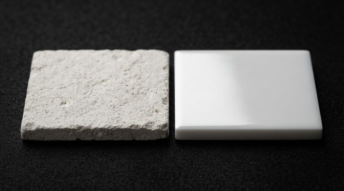
99.6% alumina thin film blanks are commonly stocked in round wafer formats (2″, 3″, 4″) and rectangular panels. Thickness typically ranges from 0.25 mm to 1.0 mm; consult the ceramic substrate thickness chart for standard options. Thinner substrates (0.25–0.38 mm) are preferred for RF hybrids where via inductance matters; thicker substrates (0.635–1.0 mm) suit power resistor networks that need mechanical rigidity.
When Not to Use 99.6% Alumina
Thick film circuits with ≥ 100 µm features. Screen-printed conductors do not benefit from the finer surface finish. Use 96% alumina and save 40–60% on substrate cost.
High-power modules above 5 W/cm². The 28–35 W/mK thermal conductivity of alumina becomes a bottleneck. Switch to AlN (170–200 W/mK) or a DBC/AMB structure for direct die-attach applications.
Mechanically loaded or vibration-heavy environments. Alumina is brittle. If your assembly will see sustained mechanical shock, consider Si3N4 AMB substrates, which offer roughly 2–3× the fracture toughness.
Cost-sensitive consumer electronics. If the circuit can tolerate FR-4 or metal-core PCB performance, ceramic is not justified.
Frequently Asked Questions
Can I get 99.6% alumina substrates with through-holes or vias?
Yes. Vias are typically laser-drilled or punched before firing, then filled with tungsten or gold metallization. Minimum via diameter depends on substrate thickness but is commonly 0.1–0.2 mm for thin film grades.
What surface finish should I specify for thin film sputtering?
Specify Ra ≤ 0.05 µm (lapped and polished) for line/space below 25 µm. For features above 25 µm, as-fired 99.6% alumina at Ra 0.15–0.25 µm may be acceptable, but yield will be lower than on a polished surface.
Does 99.6% alumina work at cryogenic temperatures?
It does. Alumina retains its mechanical strength and dielectric properties down to liquid-helium temperatures (4 K). Thermal conductivity increases significantly below 100 K, peaking near 30–40 K, per data in CoorsTek’s cryogenic property tables.
How does alumina 99.6% Al2O3 thin film ceramic handle repeated thermal cycling?
The substrate itself is extremely stable through thousands of cycles between −55 °C and +300 °C. The failure mode in thermal cycling is almost always at the metallization-to-ceramic interface, not in the bulk ceramic. Proper adhesion-layer design (Ti or Cr at 30–50 nm) is the critical factor.
Is 99.6% alumina biocompatible?
High-purity alumina is widely used in medical implants and is considered biocompatible per ISO 10993 testing. The low glass-phase content of 99.6% alumina reduces leachable ions compared to 96% grades, which is why it is preferred for implantable electronics substrates.
Next Step
If you are evaluating alumina 99.6% Al2O3 thin film ceramic for a project, request a free ceramic substrate sample kit to test surface finish and metallization adhesion with your own process. For a quotation on custom sizes or metallized substrates, contact us through the quote page with your substrate drawing and quantity.