This ceramic PCB glossary collects the terms hardware engineers, thermal engineers, and sourcing managers encounter most often when working with ceramic substrates. Each entry gives a concise definition, the context where the term matters, and a link to deeper reading where available. Bookmark this page and return to it whenever a datasheet or supplier quote uses unfamiliar shorthand.
How to Use This Glossary
Terms are arranged alphabetically. Acronyms are listed under their abbreviation (e.g., DBC, not “Direct Bonded Copper”). Where a term has a dedicated deep-dive page on this site, the first mention links to it. Property values shown here are typical ranges for orientation; always confirm against the specific grade datasheet before committing to a design.
A
Alumina (Al₂O₃)
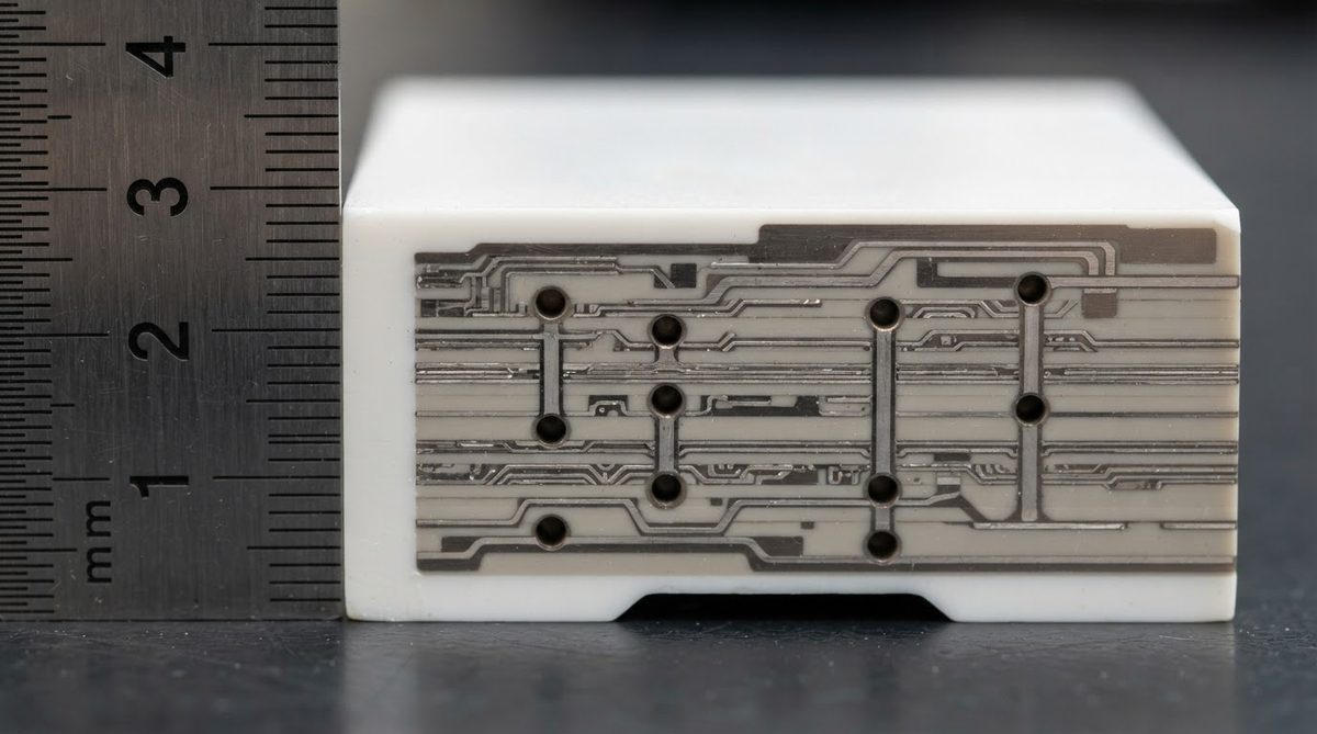
Alumina is aluminum oxide ceramic, the most widely used substrate material in ceramic PCBs. Common grades are 96% and 99.6% purity. Thermal conductivity ranges from 24–28 W/mK (96%) to 28–35 W/mK (99.6%) at 25 °C, per CoorsTek ADS-996 datasheets. Higher purity improves both thermal performance and surface finish but increases cost.
Aluminum Nitride (AlN)
Aluminum nitride is a ceramic with thermal conductivity of 170–200 W/mK at 25 °C, roughly 6–8× that of 96% alumina. It is used where high heat flux demands a thermally superior substrate, such as high-power LED modules and GaN power stages. AlN is more expensive and more sensitive to moisture than alumina.
AMB (Active Metal Brazing)
AMB is a metallization process that bonds copper foil to a ceramic substrate using a braze alloy containing an active metal, typically titanium. The braze reacts with the ceramic surface at 800–900 °C in vacuum, forming a chemical bond. AMB handles thicker copper (up to 0.8 mm or more) than DBC and works on AlN and Si₃N₄ as well as alumina.
B
Beryllia (BeO)
Beryllia is beryllium oxide ceramic, offering thermal conductivity of 250–300 W/mK at 25 °C. Warning: beryllium oxide dust is a confirmed human carcinogen and causes chronic beryllium disease. Handling, machining, and disposal require strict controls per OSHA 29 CFR 1910.1024. BeO is used only where no alternative meets the thermal requirement, primarily legacy RF and aerospace modules. See beryllia safety information before specifying this material.
Brazing
Brazing is a joining process in which a filler metal with a liquidus above 450 °C wets and bonds two surfaces without melting the base materials. In ceramic PCBs, brazing bonds copper to ceramic (as in AMB) or attaches heat sinks and leads. Vacuum or controlled-atmosphere furnaces are standard to prevent oxidation.
C
Camber
Camber is the bow or warp across a ceramic substrate, usually expressed as a ratio of deflection to diagonal length. Typical spec for 96% alumina substrates is ≤ 0.1 mm per 25 mm (per ASTM C1161 flatness guidance). Excessive camber causes solder voids during reflow.
Castellation
Castellation is a half-via at the edge of a substrate, formed by drilling or punching a via and then singulating through its center. Castellations allow a ceramic module to be soldered directly onto a host PCB like a surface-mount component. They are common in RF filter packages and sensor modules.
Ceramic Firing
Ceramic firing is the thermal process that densifies a green (unfired) ceramic body into a solid substrate. Firing temperatures range from roughly 850 °C for LTCC glass-ceramic tapes to 1,600 °C or higher for HTCC alumina. Firing profile—ramp rate, peak temperature, hold time, cooling rate—directly controls final density, shrinkage, and dimensional tolerance.
Co-Fired Ceramic
Co-fired ceramic refers to a multilayer substrate in which ceramic tape layers and printed conductor patterns are laminated and then sintered together in a single firing step. The two main families are HTCC and LTCC, distinguished by firing temperature and compatible conductor metals.
CTE (Coefficient of Thermal Expansion)
CTE is the rate at which a material expands per degree of temperature change, expressed in ppm/°C. Alumina has a CTE of approximately 7–8 ppm/°C, which is a close match to silicon (≈ 3.5 ppm/°C) and GaAs (≈ 5.7 ppm/°C) compared with FR-4 (≈ 14–17 ppm/°C). A low CTE mismatch between substrate and die reduces solder-joint fatigue during thermal cycling.
D
DBC (Direct Bonded Copper)
DBC is a process that bonds copper foil to a ceramic substrate by oxidizing the copper surface and heating the assembly to the Cu–Cu₂O eutectic point (approximately 1,065 °C). The resulting copper-oxide interlayer wets the ceramic and forms a strong bond. DBC is the dominant metallization for power-module substrates on Al₂O₃ and AlN. Typical copper thickness ranges from 0.127 mm to 0.635 mm (5–25 mil).
DCB (Direct Copper Bonding)
DCB is an alternate abbreviation for DBC. The two terms are interchangeable in industry literature. Some suppliers use DCB to distinguish their specific process variant, but the underlying chemistry is the same.
Dielectric Constant (Dk)
Dielectric constant is the relative permittivity of the substrate material, governing signal propagation speed and impedance. 96% alumina has a Dk of approximately 9.0–9.9 at 1 MHz (per Kyocera A-493 datasheet). AlN is approximately 8.5–9.0. These values are higher than FR-4 (≈ 4.2–4.5), which means trace widths for a given impedance are narrower on ceramic.
Dielectric Strength
Dielectric strength is the maximum electric field a material can withstand before breakdown, expressed in kV/mm. 96% alumina is typically rated at 10–15 kV/mm (per CeramTec Rubalit data). High dielectric strength is a primary reason ceramic substrates are specified in high-voltage power electronics.
DPC (Direct Plated Copper)
DPC is a metallization method that deposits copper onto a ceramic substrate by sputtering a thin seed layer (often Ti/Cu or Cr/Cu) and then electroplating copper to the target thickness. DPC achieves finer trace and space resolution than DBC or thick film, typically down to 30–50 µm line/space, making it suitable for high-density interconnect on ceramic.
E
ENEPIG
ENEPIG stands for Electroless Nickel / Electroless Palladium / Immersion Gold. It is a surface finish that provides solderability, wire-bondability, and corrosion resistance. The palladium barrier layer prevents the “black pad” defect associated with ENIG. Typical layer thicknesses: 3–5 µm Ni, 0.05–0.15 µm Pd, 0.03–0.08 µm Au.
ENIG
ENIG stands for Electroless Nickel / Immersion Gold. It is the most common surface finish on ceramic PCBs for soldering applications. Typical thicknesses are 3–6 µm nickel and 0.05–0.1 µm gold, per IPC-4552 revision B. ENIG provides a flat, oxidation-resistant surface but is not recommended for aluminum wire bonding.
F
Flexural Strength
Flexural strength (modulus of rupture) is the stress at which a ceramic substrate fractures under bending load, measured per ASTM C1161. 96% alumina is typically 350–400 MPa. Si₃N₄ reaches 700–900 MPa, which is why it is preferred for substrates subject to mechanical stress or thermal shock.
G
Green Tape
Green tape is unfired ceramic in thin, flexible sheet form, used as the starting material for HTCC and LTCC processes. It consists of ceramic powder, glass frit (in LTCC), organic binders, and solvents, cast into sheets by doctor-blade or tape-casting methods. After via punching, conductor printing, and lamination, the green tape stack is co-fired.
H
HTCC (High-Temperature Co-Fired Ceramic)
HTCC is a multilayer ceramic process fired at 1,500–1,600 °C. Because of the high sintering temperature, conductors must be refractory metals—typically tungsten (W) or molybdenum-manganese (Mo/Mn). HTCC substrates offer high mechanical strength, hermeticity, and dimensional stability. The trade-off is higher conductor resistivity compared with copper- or silver-based LTCC conductors.
I
Impedance
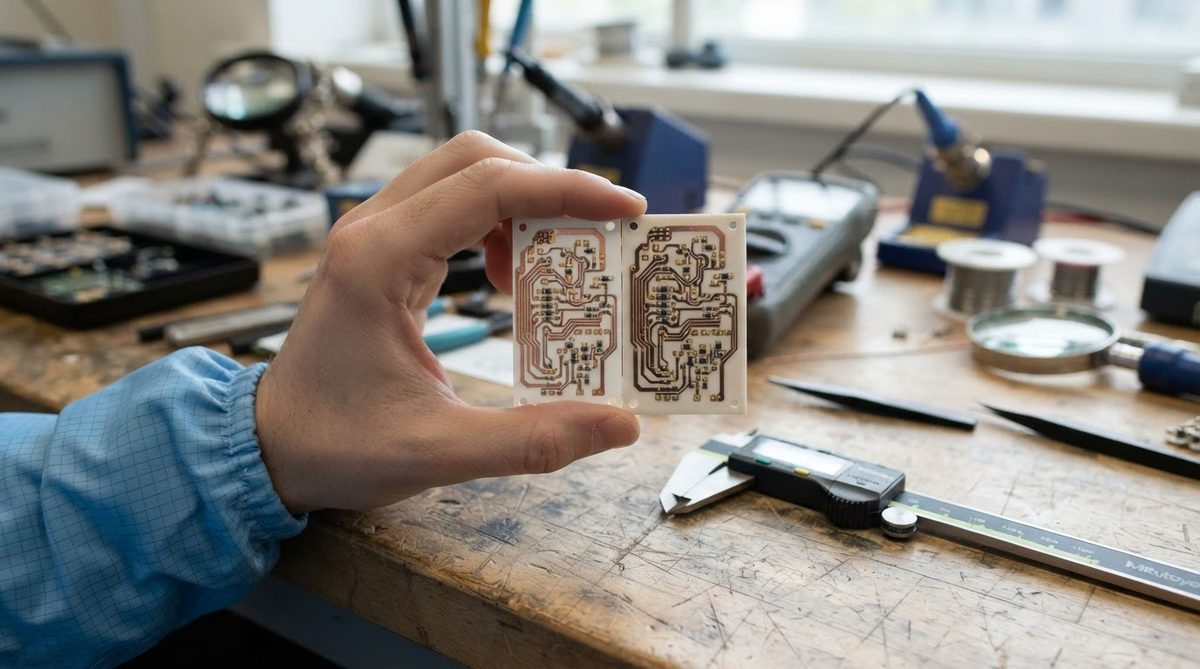
Impedance is the total opposition a circuit presents to alternating current, measured in ohms. On ceramic substrates, controlled impedance traces are designed using the substrate’s Dk, trace geometry, and ground-plane spacing. Because alumina’s Dk is roughly 9–10, traces are narrower than equivalent impedance lines on FR-4.
L
LTCC (Low-Temperature Co-Fired Ceramic)
LTCC is a multilayer ceramic process fired at 850–900 °C. The lower temperature permits silver or gold conductors, which have much lower resistivity than the tungsten used in HTCC. LTCC is widely used in RF modules, automotive radar, and miniaturized sensor packages. Typical Dk of LTCC tape systems ranges from 5.5 to 9.0 depending on the formulation.
M
Metallization
Metallization is the general term for applying conductive metal layers to a ceramic substrate. Major methods include DBC, AMB, DPC, thick film (screen-printed and fired paste), and thin film (sputtered/evaporated layers). The choice of metallization determines achievable trace resolution, current-carrying capacity, and thermal resistance.
S
Si₃N₄ (Silicon Nitride)
Silicon nitride is a ceramic with thermal conductivity of 70–90 W/mK and flexural strength of 700–900 MPa—the highest mechanical toughness among common substrate ceramics. It resists thermal-shock cracking far better than alumina or AlN, making it the preferred substrate for high-reliability power modules in EV traction inverters. It is also the most expensive of the three mainstream substrate ceramics.
Sintering
Sintering is the densification of a ceramic powder compact by heating below its melting point. Atomic diffusion at grain boundaries eliminates porosity and bonds particles together. Sintering temperature, atmosphere, and time determine final density, grain size, and mechanical properties.
Substrate
A substrate is the base insulating layer on which conductors, resistors, and components are built. In ceramic PCBs, the substrate is the fired ceramic plate itself. Substrate selection—material, thickness, surface roughness—affects every downstream electrical, thermal, and mechanical parameter of the finished board.
T
Thick Film
Thick film is a metallization process in which conductive, resistive, or dielectric pastes are screen-printed onto a fired ceramic substrate and then sintered at 850–1,000 °C. Conductor pastes are typically silver, gold, or palladium-silver. Thick film achieves line widths of roughly 100–150 µm and is cost-effective for moderate-density circuits, hybrid modules, and printed resistors.
Thin Film
Thin film is a metallization process that deposits metal layers by sputtering or evaporation in vacuum, followed by photolithographic patterning and etching. Thin film achieves line widths below 25 µm and tight resistor tolerances (± 0.1–1%). It is used for precision analog circuits, RF matching networks, and high-density interconnects on ceramic.
Thermal Conductivity
Thermal conductivity (k) is the rate at which heat passes through a material, expressed in W/mK. It is the single most referenced property when selecting a ceramic substrate for thermal management. Typical values at 25 °C: Al₂O₃ 96% → 24–28 W/mK; AlN → 170–200 W/mK; Si₃N₄ → 70–90 W/mK (per Kyocera and Maruwa datasheets).
Thermal Via
A thermal via is a plated or filled via placed directly beneath a heat source to conduct heat through the substrate to a heat sink on the opposite side. In ceramic PCBs, thermal vias can be filled with copper (in DPC) or tungsten (in HTCC), providing a low-resistance thermal path. Via fill material and diameter determine the effective thermal conductivity of the via array.
V
Via
A via is a conductive pathway through the substrate connecting metal layers on opposite sides or between internal layers. In ceramic PCBs, vias are formed by laser drilling, mechanical punching (in green tape), or CNC drilling (in fired substrates), then filled or plated with metal. Via diameter, pitch, and fill quality directly affect both electrical performance and thermal resistance.
Quick-Reference Property Table
| Material | Thermal Conductivity (W/mK) | CTE (ppm/°C) | Dk at 1 MHz | Flexural Strength (MPa) | Source |
|---|---|---|---|---|---|
| Al₂O₃ 96% | 24–28 | 7.2–8.0 | 9.0–9.9 | 350–400 | CoorsTek ADS-996, Kyocera A-493 |
| Al₂O₃ 99.6% | 28–35 | 7.5–8.2 | 9.7–10.0 | 400–450 | CoorsTek ADS-995 |
| AlN | 170–200 | 4.5–5.0 | 8.5–9.0 | 300–350 | Kyocera SH-30, Maruwa AN-200 |
| Si₃N₄ | 70–90 | 2.5–3.5 | 8.0–9.0 | 700–900 | Kyocera SN-90 |
| BeO | 250–300 | 7.5–8.5 | 6.5–7.0 | 230–250 | Materion Thermalox 995 |
Typical values for commercially available material, for comparison only. Confirm against the datasheet for your specific grade.
When This Glossary Is Not Enough
A glossary gives you the vocabulary. It does not replace material datasheets, IPC standards (IPC-2221, IPC-6012), or application-specific design guides. If you are sizing a substrate for a power module, you need thermal simulation, not a definition of thermal conductivity. If you are qualifying a finish for wire bonding, you need the IPC-4552 spec and a pull-test report, not a paragraph on ENIG.
Use this page to decode unfamiliar terms quickly, then move to the relevant deep-dive article or standard for engineering-level detail.
Frequently Asked Questions
What is the difference between DBC and AMB?
DBC bonds copper to ceramic at the Cu–Cu₂O eutectic (~1,065 °C) without a separate braze alloy. AMB uses an active-metal braze filler (containing Ti) at 800–900 °C. AMB supports thicker copper and works on AlN and Si₃N₄; DBC is simpler and lower cost on alumina.
Are HTCC and LTCC the same thing?
No. HTCC fires at 1,500–1,600 °C and uses tungsten or moly conductors. LTCC fires at 850–900 °C and uses silver or gold. The choice affects conductor resistivity, material cost, and compatible passive components.
Can I get controlled impedance on a ceramic PCB?
Yes. Impedance is controlled by trace width, substrate thickness, Dk, and ground-plane spacing, just as on FR-4. Because alumina’s Dk is roughly 9–10, traces will be narrower for the same impedance target. Thin-film and DPC processes offer the tightest geometry control.
Why does CTE matter for ceramic substrates?
A large CTE mismatch between the substrate and a bonded die or solder joint causes thermomechanical stress during temperature cycling. Ceramic substrates have CTEs of 2.5–8 ppm/°C, much closer to semiconductor die (3–6 ppm/°C) than FR-4 (14–17 ppm/°C). This reduces solder fatigue and improves long-term reliability.
Is beryllia still used in new designs?
Rarely. BeO’s thermal conductivity (250–300 W/mK) is unmatched, but its toxicity hazard limits use to legacy RF and aerospace applications where no substitute exists. AlN (170–200 W/mK) covers most high-performance needs without the health and regulatory burden.
What does “green tape” mean in ceramic manufacturing?
Green tape is unfired ceramic sheet, flexible enough to punch, print, and laminate. It becomes rigid only after co-firing. The term “green” refers to the unfired state, not the color, though many tapes happen to look greenish or white.