What Is DCB? A Clear DCB Definition
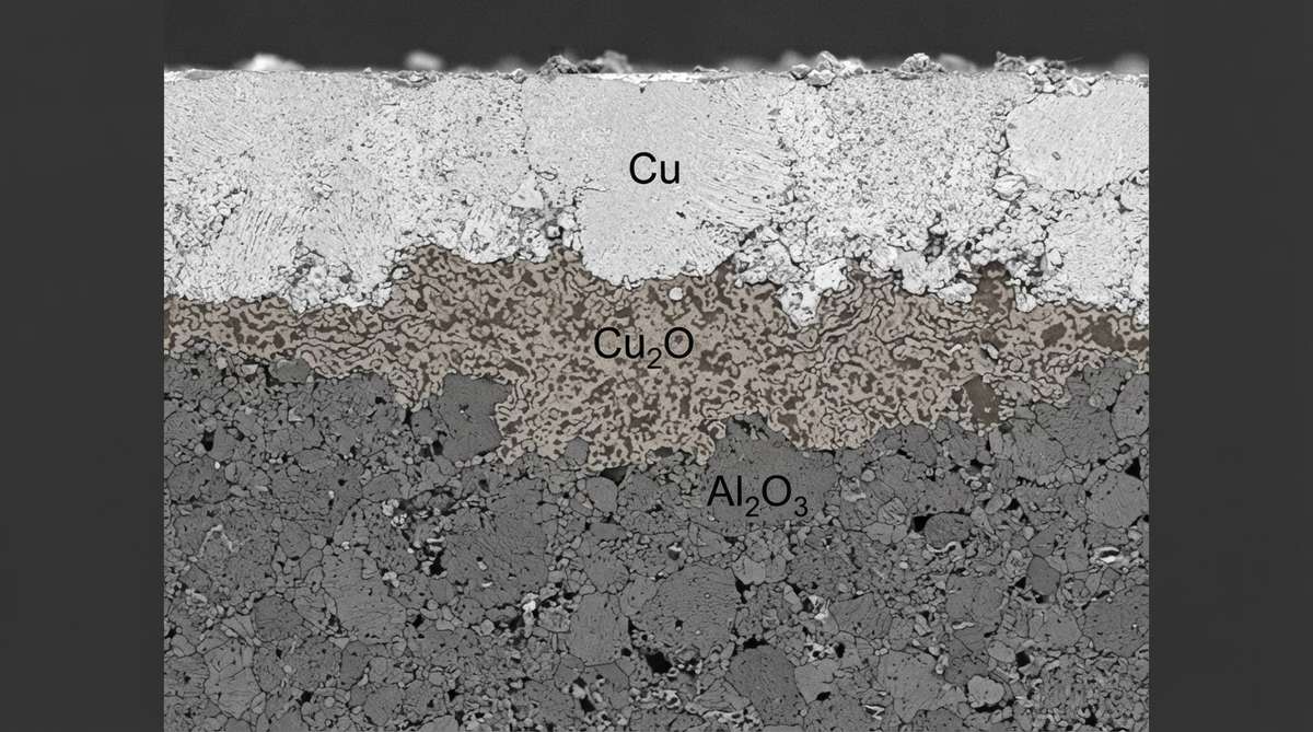
DCB (Direct Copper Bond) is a high-temperature process that bonds a sheet of copper directly to an oxide-based ceramic substrate—typically Al₂O₃ or AlN—by forming a thin copper-oxide eutectic layer at the interface. Understanding the DCB definition starts with this core mechanism: the bond forms at approximately 1065–1083 °C, just below the melting point of copper (1085 °C), producing a metallized ceramic with copper layers thick enough (typically 0.1–0.6 mm) to carry high currents and spread heat effectively.
The term is also written as DBC (Direct Bond Copper). Both abbreviations refer to the same process, and the DCB definition applies identically regardless of which acronym a datasheet uses.
How the DCB Process Works
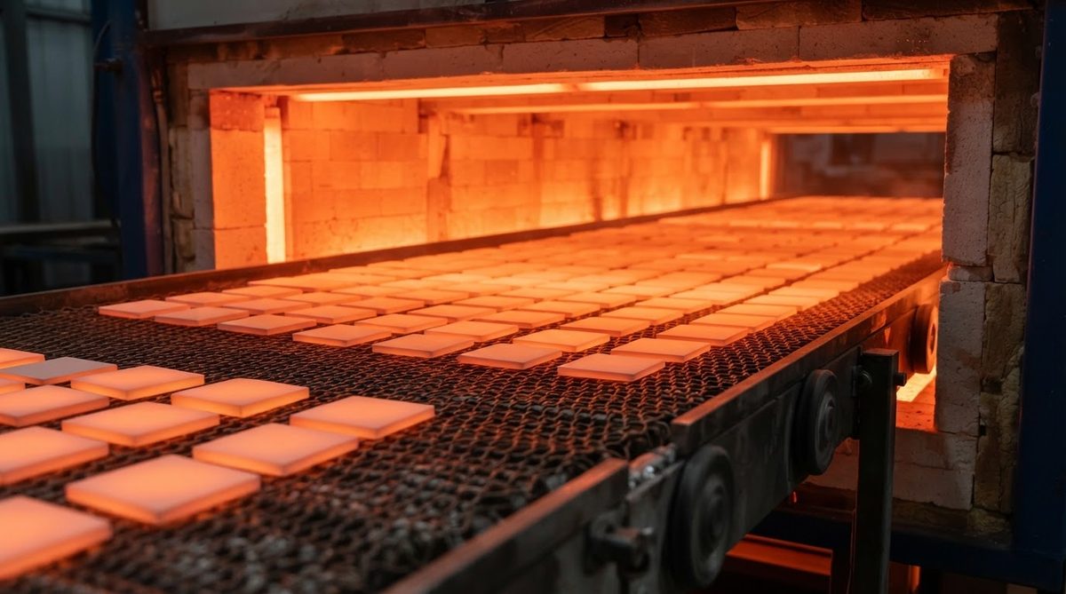
- Surface preparation. The ceramic substrate is cleaned and, for Al₂O₃, a controlled oxidation step ensures a thin oxide interface layer.
- Copper foil placement. Pre-cut copper foil is placed on one or both faces of the ceramic.
- High-temperature bonding. The assembly is heated in a nitrogen atmosphere with a small, controlled amount of oxygen to ~1065–1075 °C. A Cu–Cu₂O eutectic liquid forms and wets the ceramic surface.
- Cooling. As the assembly cools, the eutectic solidifies, creating a strong metallurgical bond between the copper and the ceramic.
- Etching. Standard photolithography and chemical etching pattern the copper into circuit traces.
Because the DCB bond relies on a copper-oxide eutectic, the process works best with oxide ceramics. Non-oxide substrates such as Si₃N₄ are typically metallized using AMB (Active Metal Brazing) instead, which uses a titanium-containing braze alloy to wet the ceramic. This distinction is central to the practical DCB definition: it is an oxide-ceramic-specific bonding method.
Typical DCB Substrate Properties
| Parameter | Value | Unit | Condition / Notes |
|---|---|---|---|
| Ceramic material | Al₂O₃ 96 % or AlN | — | Oxide ceramics preferred |
| Copper thickness | 0.1–0.6 | mm | Per side; 0.3 mm is common |
| Ceramic thickness | 0.25–1.0 | mm | 0.38 and 0.63 mm standard |
| Bond strength | ≥ 4 | N/mm | Peel test, per manufacturer data |
| Thermal conductivity (Al₂O₃ 96 %) | 24–28 | W/mK | At 20 °C |
| Thermal conductivity (AlN) | 170–200 | W/mK | At 20 °C |
| Max continuous use temperature | ~800 | °C | Limited by copper oxidation in air |
Typical values for commercially available material, for comparison only. Confirm against the datasheet for your specific grade.
These numbers show why the DCB definition matters in practice: no other single-step metallization method delivers copper this thick with a direct metallurgical bond to ceramic, which is why DCB substrates dominate high-power thermal paths.
Where DCB Substrates Are Used
DCB substrates dominate in power electronics modules—IGBT modules, SiC MOSFET packages, and high-power LED bases—where thick copper is needed for current carrying capacity and heat spreading. The die attach pad on a DCB substrate can handle direct soldering of bare semiconductor die.
When DCB Is Not the Right Choice
DCB is not suited for fine-line RF circuits or high-density interconnects. Minimum trace widths are typically 0.15–0.2 mm after etching, far coarser than thin-film or DPC processes. For circuits requiring traces below 50 µm or multi-layer routing, LTCC or thin-film metallization is a better fit. DCB also adds cost and complexity compared to thick-film screen printing when copper thickness above 0.1 mm is not needed.
FAQ
Is DCB the same as DBC?
Yes. DCB (Direct Copper Bond) and DBC (Direct Bond Copper) are two abbreviations for the identical process. The DCB definition covers both terms equally; industry usage varies by region and manufacturer.
Can DCB be applied to Si₃N₄ substrates?
No. The DCB eutectic bond requires an oxide ceramic surface. Silicon nitride substrates are metallized using Active Metal Brazing (AMB), which uses a reactive Ti-containing alloy to wet non-oxide ceramics.
What copper thickness is standard for DCB?
Most DCB suppliers offer copper from 0.1 mm to 0.6 mm per side. The 0.3 mm thickness is the most common choice, balancing current capacity, thermal spreading, and CTE-induced stress on the ceramic.
Does the ceramic crack during thermal cycling?
Thick copper on thin ceramic creates CTE mismatch stress. Proper design—symmetric copper on both sides, controlled copper thickness relative to ceramic thickness, and edge dimpling—reduces crack risk. Qualification typically follows power-cycling standards such as IEC 60749-34.