Metallization is the process of depositing or bonding a conductive metal layer onto a non-conductive ceramic substrate to form circuit traces, bond pads, ground planes, or thermal dissipation paths. Understanding this metallization definition is essential for anyone designing or sourcing ceramic PCBs, because it is the step that turns a blank ceramic piece into a functional circuit board. Without it, there is no way to route current, attach components, or move heat laterally to a sink.
Metallization Definition and Why It Matters on Ceramic PCBs
In the simplest terms, the metallization definition refers to any method that places a metal film or foil onto a non-metallic surface. On ceramic PCBs, bare substrates such as Al₂O₃, AlN, and Si₃N₄ are electrical insulators. The metallization layer is what defines trace geometry, adhesion strength, solderability, and long-term reliability of the finished board.
Key functions that metallization provides on a ceramic PCB include:
- Electrical routing — forming signal traces and ground planes that carry current across the insulating substrate.
- Component attachment — creating solderable bond pads for die attach, wire bonding, or SMT reflow.
- Thermal management — spreading heat laterally through a high-conductivity copper layer toward a heat sink or housing.
- Hermetic sealing — enabling brazed or soldered lid-seal rings on packages that require moisture or gas barriers.
Common Metallization Methods
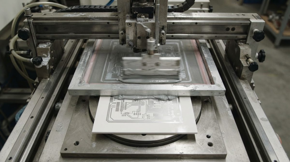
| Method | Typical metals | Line/space capability | Key trait |
|---|---|---|---|
| Thick film (screen print + fire) | Ag, Au, Ag-Pd, Ag-Pt | ≥ 100 µm / 100 µm | Low cost, mature process |
| Thin film (sputter / evaporate + etch) | Ti/Pt/Au, Ti/Cu/Au, Cr/Ni/Au | ≥ 10 µm / 10 µm | Finest resolution, tightest tolerances |
| DPC (direct plated copper) | Cu (sputtered seed + electroplated) | ≥ 20 µm / 20 µm | Good balance of resolution and thermal performance |
| DBC (direct bond copper) | Cu foil (oxidation bonded) | ≥ 200 µm / 200 µm | Thick copper (150–600 µm) for high-current power modules |
| AMB (active metal brazing) | Cu foil (brazed with Ti-containing filler) | ≥ 200 µm / 200 µm | Strongest bond; preferred for Si₃N₄ and AlN power substrates |
Typical values for commonly available processes, for comparison only. Confirm against the datasheet for your specific grade.
Choosing the Right Metallization Process
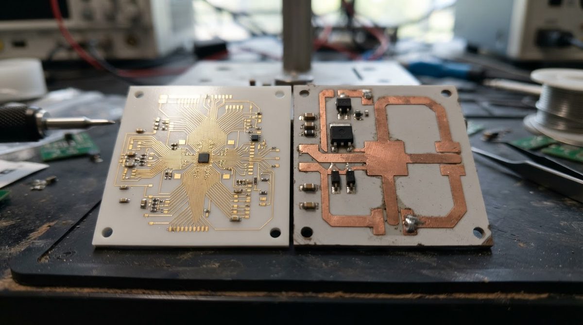
The right metallization method depends on three factors: required trace resolution, current-carrying capacity, and operating temperature. Thick-film metallization works well for hybrid circuits with modest density. Thin film and DPC suit RF and sensor applications where fine lines and tight impedance control matter. DBC and AMB handle the heavy copper needed in IGBT and SiC power modules.
Adhesion strength also varies by metallization technique. DBC and AMB create a direct ceramic-to-copper bond that survives thousands of thermal cycles per JEDEC JESD22-A104. Thick-film adhesion depends on the glass frit in the paste and the sintering process used during firing.
FAQ
Can you metallize any ceramic material?
Most engineering ceramics—Al₂O₃, AlN, Si₃N₄, ZrO₂—can be metallized, but each requires a matched process. AlN, for example, needs an oxidation or activation step before DBC bonding because bare AlN does not wet copper oxide directly.
Does metallization affect thermal resistance?
Yes. A thick copper metallization layer (300 µm via DBC) spreads heat laterally and lowers overall junction-to-case thermal resistance. A thin-film metallization of 1–5 µm contributes negligible thermal spreading but adds almost no thickness to the stackup.
Is metallization the same as plating?
Plating (electroplating or electroless plating) is one metallization technique, but the metallization definition is broader. It covers sputtering, evaporation, screen printing, brazing, and direct bonding—any method that puts metal onto a non-metallic surface.