A castellation is a plated half-via exposed at the edge of a printed circuit board, forming a semicircular or half-moon metallic contact. Understanding the castellation definition matters because these edge contacts let one board—typically a small module—be surface-mounted directly onto a larger host PCB by soldering through the exposed half-cylinder pads. The castellation definition applies equally to FR-4 and ceramic substrates, though ceramic boards demand tighter process control during singulation to avoid chipping.
How Castellations Are Made
The manufacturing sequence is straightforward. Full vias are drilled or punched along the board outline, plated with copper (and often finished with a protective surface coating), then the panel is routed or scored through the center of each via. The result is a row of half-cylinder metallic pads along the board edge—each one a castellation by definition.
On ceramic substrates produced by HTCC or LTCC processes, via holes are punched into green-tape layers before sintering. After firing and metallization, the panel is diced through the via centers using a diamond saw or laser, leaving clean castellated edges.
Why the Castellation Definition Matters on Ceramic Boards
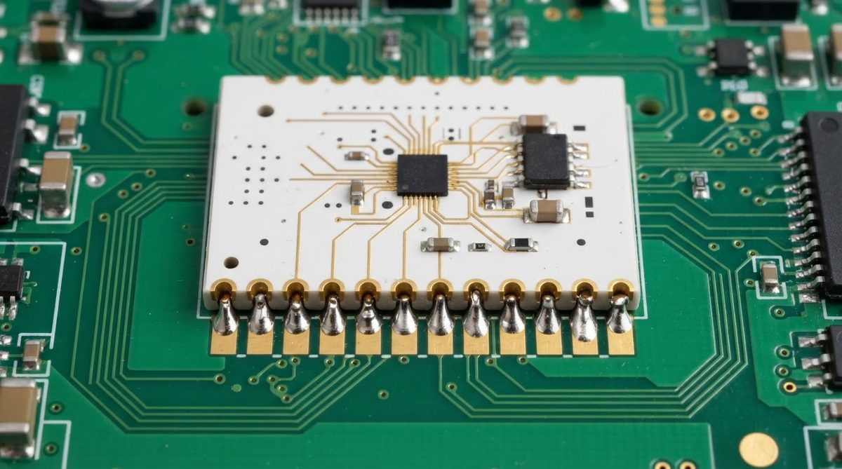
Ceramic modules are common in RF, sensor, and power applications where the module must be reflow-soldered onto a host board. Castellations provide three things at once: an electrical connection, a mechanical anchor, and a thermal path from the module into the host PCB. Because ceramic is rigid and cannot flex, a reliable solder joint at the castellation is critical to surviving thermal cycling.
Typical castellation diameters on ceramic boards range from 0.3 mm to 1.0 mm before halving, depending on substrate thickness and the via process used. Smaller castellations demand tighter routing tolerances to avoid chipping the brittle ceramic edge.
Design Tips for Castellated Ceramic Modules
- Keep castellations at least 0.5 mm from board corners to reduce fracture risk during singulation.
- Specify a solderable finish—ENIG or electroplated nickel/gold—on the castellation surfaces to ensure wettability.
- Match the CTE of the module substrate to the host board as closely as practical; a large mismatch concentrates stress at the castellation joints during reflow and thermal cycling.
- On the host-board footprint, extend the landing pads slightly beyond the castellation semicircle so solder fillets are visible for inspection.
Castellation vs. Standard Edge Plating
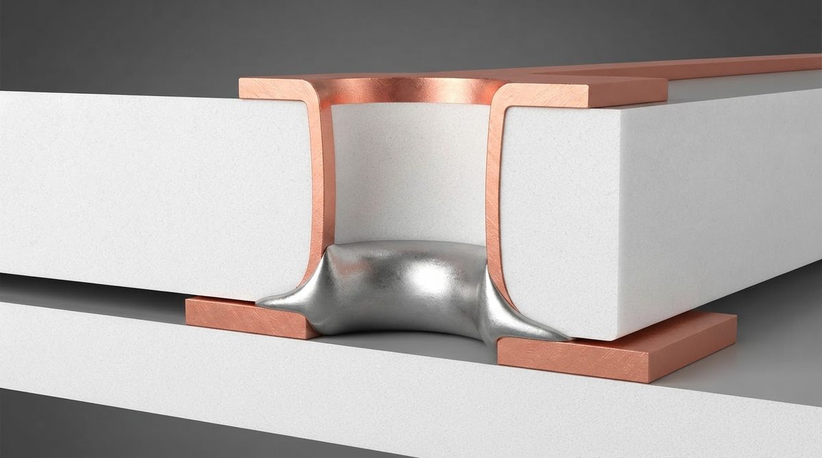
Edge plating coats a flat board edge with metal, creating a continuous strip. A castellation, by contrast, is a discrete semicircular contact at a specific location. Castellations carry individual signals or power nets; edge plating is typically used for shielding or grounding an entire board perimeter. The two serve different purposes and should not be confused in a specification. Knowing the precise castellation definition helps you call out the correct feature on your drawing.
Frequently Asked Questions
What is the simplest castellation definition for a PCB?
A castellation is a plated half-via at the board edge that acts as a solderable contact pad. It is created by drilling or punching a full via along the board outline and then cutting through its center during singulation, leaving a semicircular metallic surface.
Can castellations be used on both FR-4 and ceramic PCBs?
Yes. The castellation definition is the same regardless of substrate material. However, ceramic substrates require diamond-saw or laser dicing instead of mechanical routing, and tighter tolerances are needed to prevent edge chipping.
How small can a castellation be on a ceramic board?
Castellation diameters before halving typically range from 0.3 mm to 1.0 mm on ceramic substrates. The lower limit depends on substrate thickness, via plating capability, and the precision of the dicing equipment. Smaller castellations increase the risk of edge fracture.
Do castellations need a special surface finish?
Castellations should have a solderable finish such as ENIG or electroplated nickel/gold to ensure reliable wetting during reflow. Bare copper castellations oxidize quickly and can cause poor solder joints, especially on modules that may sit in storage before assembly.