Impedance Definition: What It Means in Circuit and PCB Terms
The standard impedance definition is straightforward: impedance is the total opposition an electrical circuit presents to alternating current (AC), expressed in ohms (Ω). It combines three components — resistance (R), inductive reactance (XL), and capacitive reactance (XC). Unlike pure DC resistance, impedance is frequency-dependent and is represented as a complex number: Z = R + j(XL − XC).
In PCB design, the impedance definition usually narrows to characteristic impedance (Z₀), the instantaneous ratio of voltage to current along a transmission line. For most high-speed and RF boards, characteristic impedance targets fall between 25 Ω and 100 Ω, with 50 Ω being the most common single-ended value per IPC-2141A.
Why the Impedance Definition Matters on Ceramic Substrates
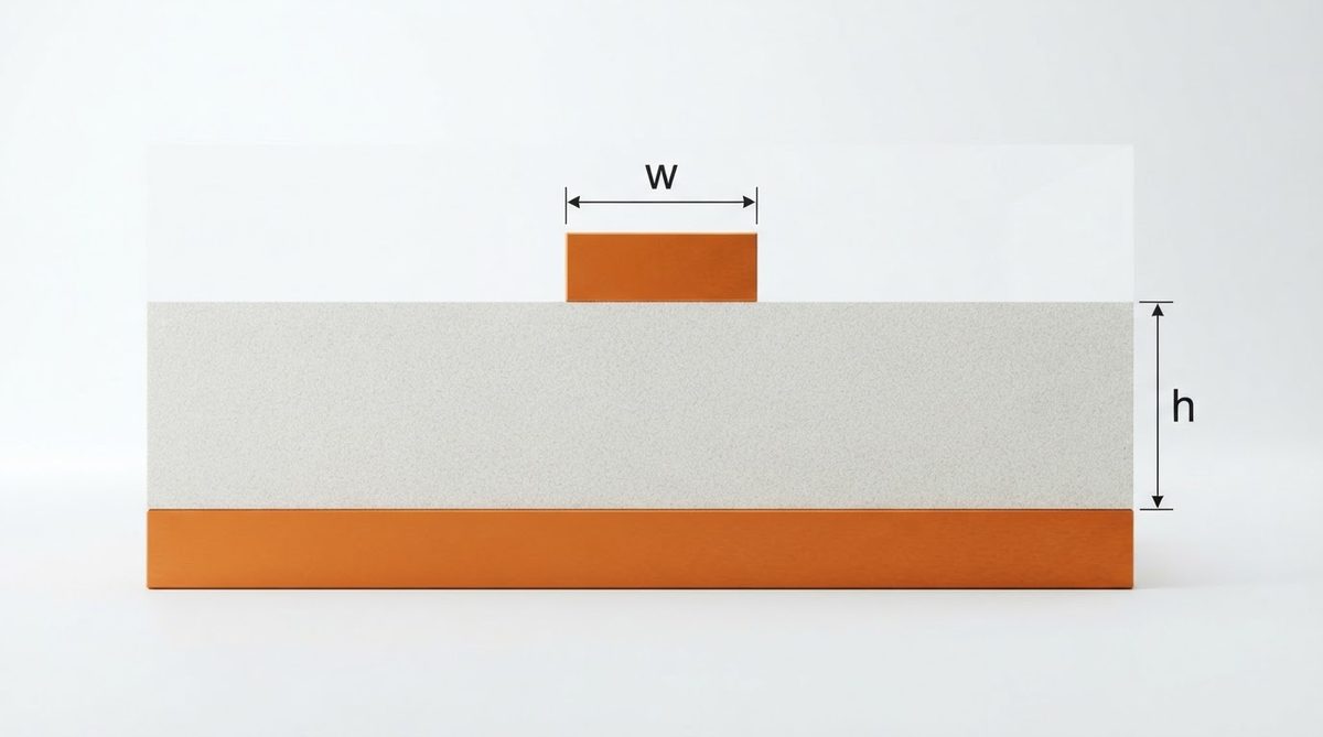
Ceramic substrates such as Al₂O₃ (96 %) have a dielectric constant (Dk) of roughly 9.0–9.9 at 1 MHz, significantly higher than FR-4’s 4.2–4.5. A higher Dk pulls characteristic impedance down for the same trace geometry. Engineers targeting 50 Ω on alumina therefore need narrower traces or thicker dielectric layers compared to FR-4.
Surface roughness also plays a role. Conductor losses increase with roughness, especially above 1 GHz, altering the effective impedance seen by a signal. Thin-film metallisation on polished ceramic can hold tighter impedance tolerances (± 5 % or better) than thick-film processes because the conductor edges and dielectric interface are smoother and more uniform.
Key Factors That Control Impedance
Several physical parameters determine the characteristic impedance of a ceramic PCB trace. Understanding each one is essential for applying the impedance definition to a real layout:
- Dielectric constant (Dk): Higher Dk lowers Z₀. Ceramic Dk values range from about 6.0 (AlN) to 9.9 (Al₂O₃ 96 %).
- Trace width: A wider trace reduces Z₀. Typical ceramic trace widths span 25 µm to 500 µm.
- Dielectric thickness: A thicker dielectric raises Z₀. Ceramic substrates commonly range from 0.25 mm to 1.0 mm.
- Conductor thickness: Has a minor effect; thicker conductors slightly lower Z₀. Values range from 1 µm (thin film) to 300 µm (DBC).
- Ground plane proximity: A closer ground plane lowers Z₀, set primarily by substrate thickness.
| Factor | Effect on Z₀ | Typical Range on Ceramic |
|---|---|---|
| Dielectric constant (Dk) | Higher Dk → lower Z₀ | 6.0 (AlN) – 9.9 (Al₂O₃ 96 %) |
| Trace width | Wider trace → lower Z₀ | 25 µm – 500 µm |
| Dielectric thickness | Thicker dielectric → higher Z₀ | 0.25 mm – 1.0 mm |
| Conductor thickness | Minor effect; thicker → slightly lower Z₀ | 1 µm (thin film) – 300 µm (DBC) |
| Ground plane proximity | Closer ground → lower Z₀ | Set by substrate thickness |
Values are representative of commercially available ceramic substrates. Confirm against the datasheet for your specific grade.
Quick Worked Example: Applying the Impedance Definition
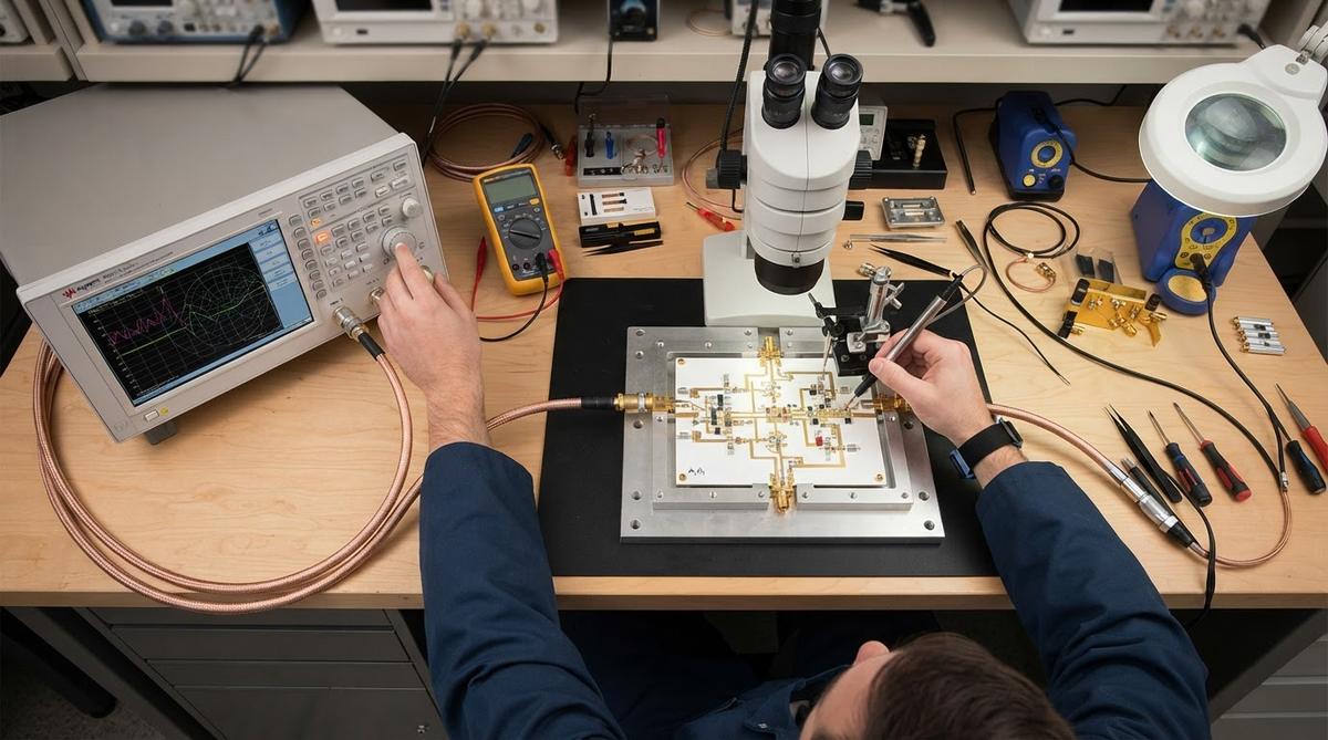
For a microstrip on 0.635 mm thick 96 % Al₂O₃ (Dk ≈ 9.8 at 10 GHz) targeting 50 Ω, a 2-D field solver yields a trace width of approximately 0.58 mm. The same 50 Ω target on 0.635 mm FR-4 (Dk ≈ 4.3) would need roughly 1.2 mm. This narrower trace is an advantage for dense RF layouts but demands tighter laser-drilled via registration.
Enter your substrate thickness, Dk, and target Z₀ below to see how trace width changes across materials.
FAQ
Is impedance the same as resistance?
No. Resistance opposes DC and AC equally, while the impedance definition includes reactive components that vary with frequency. At DC (0 Hz), impedance equals resistance.
What impedance tolerance can a ceramic PCB hold?
Thin-film processes on polished alumina routinely achieve ± 5 % or better. Thick-film processes are typically ± 10 % due to greater line-edge variation.
Does a higher dielectric constant always hurt impedance control?
Not necessarily. A higher Dk shrinks the required trace width, which saves board area. The trade-off is that manufacturing tolerances in trace width have a proportionally larger effect on Z₀, making the impedance definition harder to meet in practice without tight process control.