The right surface finishes ceramic PCB designers select protect exposed metallization from oxidation and determine solderability, wire-bondability, contact resistance, and shelf life. Choosing the wrong finish can mean failed solder joints, black-pad defects, or unnecessary cost. This guide compares every finish commonly applied to alumina, aluminum nitride, and other ceramic substrates so you can match the finish to your assembly process and operating environment.
Key Takeaways
- ENIG (3–5 µm Ni / 0.05–0.15 µm Au) is the default choice for most ceramic PCB applications—flat, solderable, and shelf-stable for 12+ months.
- ENEPIG adds a 0.05–0.15 µm palladium barrier that eliminates black-pad risk and supports gold, aluminum, and copper wire bonding on a single finish.
- Immersion silver (0.15–0.40 µm Ag) offers the lowest insertion loss for RF ceramic boards but tarnishes within 6–12 months without sealed packaging.
- OSP is the cheapest finish and works well for single-reflow assemblies, but its thin organic layer degrades above 260 °C and limits shelf life to about 6 months.
- Electrolytic hard gold (0.5–2.5 µm Au over 2–5 µm Ni) is required for high-cycle contact pads and thermosonic gold wire bonding but costs 3–8× more than ENIG per unit area.
What Each Surface Finish Does on a Ceramic Substrate
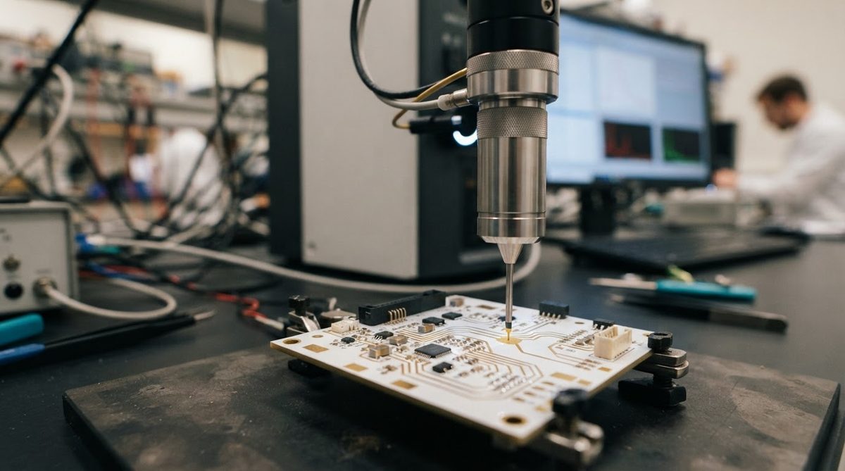
A surface finish serves two functions: it keeps the solderable or bondable metal from oxidizing before assembly, and it participates in the metallurgical joint during soldering or wire bonding. On ceramic PCBs the substrate is inert—alumina and AlN do not absorb moisture or outgas organics the way FR-4 does—so finish adhesion depends almost entirely on the underlying metallization (typically sputtered or plated Cu, or thick-film Ag/Au). This means some finishes that work fine on organic boards behave differently on ceramics. OSP, for example, bonds to the copper surface through a chemical reaction with Cu ions; on a DPC substrate with sputtered Cu, the reaction kinetics can differ from electroplated Cu on FR-4, sometimes producing thinner or less uniform coatings.
Understanding the ceramic PCB manufacturing process helps clarify why finish selection matters more here than on organic boards. Ceramic substrates often see higher reflow temperatures (some high-temp solders exceed 300 °C), more thermal cycles in service, and tighter wire-bond pull-strength requirements. The surface finishes ceramic PCB manufacturers offer must survive all of that.
Surface Finishes Ceramic PCB Comparison Table
| Finish | Typical Thickness | Shelf Life (sealed) | Solderable | Au Wire Bond | Al Wire Bond | Relative Cost | Key Limitation |
|---|---|---|---|---|---|---|---|
| ENIG | 3–5 µm Ni / 0.05–0.15 µm Au | 12+ months | Yes | Marginal | No | 1× (baseline) | Black-pad risk (Ni hyper-corrosion) |
| ENEPIG | 3–5 µm Ni / 0.05–0.15 µm Pd / 0.03–0.10 µm Au | 12+ months | Yes | Yes | Yes | 1.3–1.6× | Tighter process control needed |
| EPIG | 0.05–0.15 µm Pd / 0.03–0.08 µm Au (no Ni) | 6–12 months | Yes | Yes | Limited | 1.2–1.5× | Less common; fewer qualified suppliers |
| Immersion Ag | 0.15–0.40 µm Ag | 6–12 months | Yes | No | No | 0.7–0.9× | Tarnish; creep corrosion in sulfur environments |
| Immersion Au | 0.03–0.10 µm Au (direct on Cu) | 12+ months | Yes | No | No | 1.0–1.3× | Thin; not bondable |
| OSP | 0.2–0.5 µm organic | ~6 months | Yes (1–2 reflows) | No | No | 0.3–0.5× | Degrades >260 °C; short shelf life |
| Immersion Sn | 0.8–1.2 µm Sn | 6–9 months | Yes | No | No | 0.5–0.7× | Tin whisker risk; limited high-temp use |
| Electrolytic Hard Au | 0.5–2.5 µm Au / 2–5 µm Ni | 24+ months | Yes (selective) | Yes | Yes | 3–8× | Requires plating bus; high cost |
Typical values for commercially available finishes, for comparison only. Confirm against the datasheet for your specific chemistry and supplier. Thickness ranges per IPC-4552 (ENIG), IPC-4556 (ENEPIG), and IPC-4553 (immersion Ag).
ENIG on Ceramic PCBs
ENIG finish for ceramic boards remains the most widely specified surface finish for ceramic circuit boards. The nickel barrier (3–5 µm per IPC-4552B) prevents copper diffusion into the gold layer and provides a hard, flat surface for fine-pitch component placement. The thin immersion gold (0.05–0.15 µm) protects the nickel from oxidation until reflow.
The main risk is black pad—a hyper-corrosion of the nickel surface during the immersion gold bath that creates a brittle, phosphorus-rich layer. On ceramic substrates, black pad is less frequent than on FR-4 because the substrate does not outgas volatiles that can disrupt the plating bath, but it still occurs if bath chemistry drifts. Specify a minimum nickel phosphorus content of 7–9 wt% (mid-phos) and require cross-section verification on first articles.
Worked Example: ENIG Solder-Joint Reliability
Consider a 0.5 mm pitch QFN on a 96% alumina DPC board, reflowed with SAC305 at a peak of 245 °C. The intermetallic formed is (Cu,Ni)₆Sn₅. After 1,000 thermal cycles (−40 °C to +125 °C, 15-min dwell), shear strength typically remains above 80% of the initial value—provided the nickel layer is ≥3 µm and free of black-pad defects. If your application demands >2,000 cycles at that range, consider ENEPIG instead, because the palladium interlayer slows intermetallic growth.
ENEPIG: The Universal Finish
ENEPIG finish inserts a thin palladium layer (0.05–0.15 µm per IPC-4556) between nickel and gold. This palladium acts as a diffusion barrier that virtually eliminates black-pad risk and enables gold wire bonding, aluminum wire bonding, and soldering on the same pad set. For ceramic PCBs used in semiconductor packaging—where a die is wire-bonded to the substrate and passives are soldered on the same board—ENEPIG is often the only finish that satisfies both requirements without selective plating.
The trade-off is cost (roughly 30–60% more than ENIG) and process sensitivity. The Pd bath must be tightly controlled; too thick a palladium layer can impair solder wetting. Specify the palladium thickness window explicitly on your fabrication drawing, and require the supplier to measure it with XRF on every lot.
Immersion Silver for RF Ceramic Boards
Immersion silver deposits 0.15–0.40 µm of silver directly onto copper per IPC-4553. Silver has the highest electrical conductivity of any metal (6.30 × 10⁷ S/m at 20 °C), which translates to the lowest skin-effect losses at microwave frequencies. For ceramic substrates used in 5G mmWave front-ends, radar modules, or satellite transponders, immersion silver can reduce insertion loss by 0.01–0.03 dB/cm at 28 GHz compared to ENIG, because the nickel layer in ENIG is ferromagnetic and lossy.
The weakness is tarnish. Silver reacts with atmospheric sulfur compounds to form Ag₂S, which degrades solderability. Boards must be vacuum-sealed with desiccant immediately after finishing and used within 6–12 months. In service, conformal coating or hermetic sealing is essential. For boards that need long warehouse storage, this finish is a poor fit. Understanding impedance control on ceramic substrates helps you decide whether the RF gain from silver justifies the handling constraints.
OSP on Ceramic Substrates
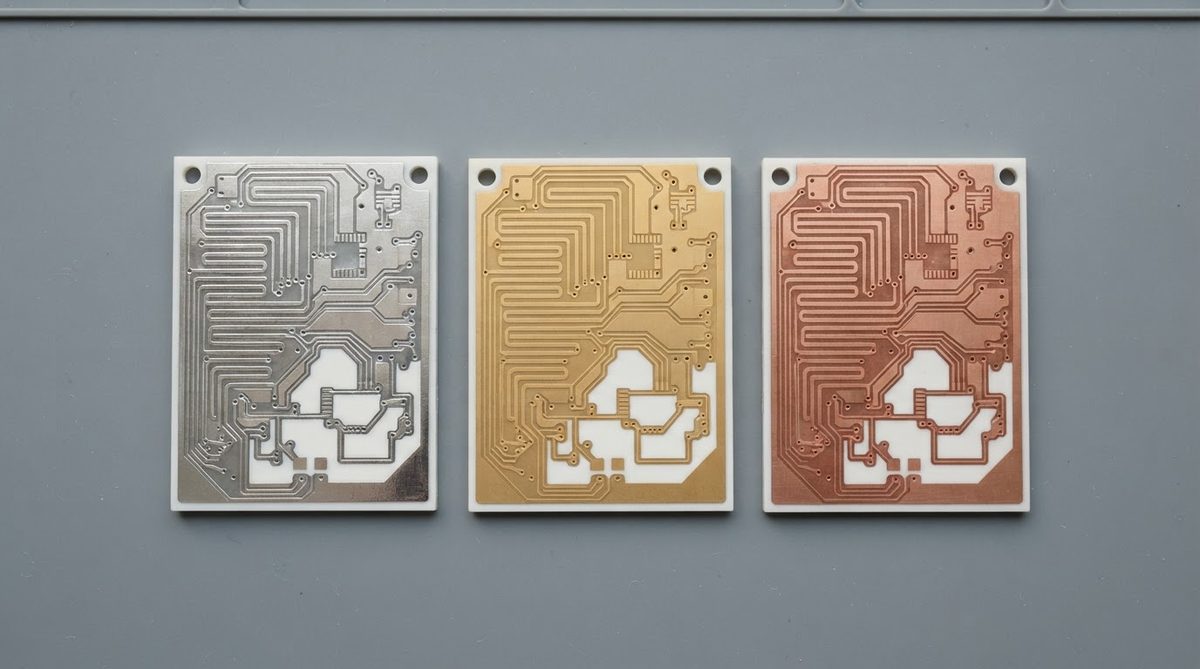
OSP finish applies a thin (0.2–0.5 µm) organic solderability preservative—typically a benzimidazole compound—to bare copper. It is the cheapest among all surface finishes ceramic PCB fabricators offer and produces an extremely flat, coplanar surface. On ceramic PCBs, OSP works well for high-volume LED packages and simple single-reflow assemblies where boards go straight from fabrication to SMT within weeks.
OSP has clear limits. The organic layer begins to degrade above 260 °C, so it tolerates only one or two lead-free reflow passes. It is invisible under AOI, making AOI inspection of pad coverage harder. And it offers no protection for wire-bond pads. If your ceramic board needs rework or multiple reflow cycles, choose a metallic finish instead.
Immersion Gold (Direct) and Immersion Tin
Immersion gold deposits a thin gold layer (0.03–0.10 µm) directly onto copper without a nickel barrier. It provides good oxidation resistance and a flat surface, but the gold is too thin for wire bonding. It suits applications where solderability and long shelf life matter more than bondability—test fixtures, for instance, or connector pads that see repeated mating cycles at low force.
Immersion tin deposits 0.8–1.2 µm of tin onto copper. It offers excellent solderability and a low cost, but tin whisker growth is a concern in high-reliability applications per JEDEC JESD201. Tin whiskers can reach 50–100 µm within months in humid environments, potentially shorting fine-pitch traces. For aerospace or medical ceramic boards, immersion tin is generally avoided.
Electrolytic Hard Gold and Selective Plating
When a ceramic PCB must support thermosonic gold wire bonding with pull strengths above 5 gf (per MIL-STD-883, Method 2011), electrolytic hard gold over nickel is the standard. Thickness is typically 0.5–1.25 µm Au for wire bonding and up to 2.5 µm for high-cycle contact pads (e.g., test sockets rated for >100,000 insertions). The nickel underlayer is 2–5 µm of electrolytic nickel, which is denser and more uniform than electroless nickel.
The cost penalty is significant—3–8× the cost of ENIG per unit area, depending on gold thickness and pad coverage. Selective plating (masking solder pads and plating only bond pads) reduces gold consumption but adds a masking step. For hybrid modules where some pads are soldered and others are wire-bonded, selective hard gold on bond pads plus ENIG or ENEPIG on solder pads is a common and cost-effective approach.
How to Choose the Right Surface Finishes Ceramic PCB Projects Need
Start with your assembly process, then filter by environment and cost.
- Wire bonding required? If gold wire: ENEPIG or electrolytic hard gold. If aluminum wire: ENEPIG only (among chemical finishes). If no bonding: proceed to step 2.
- Multiple reflow passes or rework? If yes, rule out OSP. ENIG, ENEPIG, or immersion gold are suitable. If you anticipate ceramic PCB rework, a metallic finish is mandatory.
- RF performance critical above 10 GHz? Immersion silver gives the lowest loss. EPIG is an alternative if tarnish is a concern.
- Shelf life >12 months needed? Rule out immersion silver (without hermetic packaging) and OSP. ENIG and ENEPIG are safe choices.
- Cost the primary driver? OSP for single-reflow; immersion tin if whisker risk is acceptable; immersion silver if RF loss matters.
Enter your substrate material, metallization type, and assembly method below to see which surface finishes ceramic PCB configurations support and how they affect thermal derating at your operating temperature.
[pcb_calc type=”smith-chart”]
When NOT to Use a Particular Finish
- Do not use ENIG if you need aluminum wire bonding—the nickel surface forms brittle Al-Ni intermetallics.
- Do not use OSP on boards stored longer than 6 months, boards reflowed more than twice, or boards operating above 260 °C continuously.
- Do not use immersion silver in environments with sulfur-bearing gases (industrial controls near paper mills, volcanic monitoring equipment) unless the board is hermetically sealed.
- Do not use immersion tin in Class 3 high-reliability assemblies per IPC-6012 where tin whisker risk is unacceptable (aerospace, implantable medical).
- Do not use electrolytic hard gold on solder pads. Gold thickness above 0.5 µm causes gold embrittlement in tin-based solder joints. Use selective plating to keep gold off solder pads.
Frequently Asked Questions
Can you solder directly to a ceramic substrate without any finish?
No. Bare copper oxidizes within hours in ambient air, and the oxide layer prevents solder wetting. Even thick-film silver or gold metallization benefits from a finish to maintain consistent solderability over storage. The only exception is immediate assembly in a nitrogen-inerted reflow oven within the same day as metallization.
Does the surface finish affect thermal conductivity of the ceramic PCB?
Negligibly. The finish layer is 0.05–5 µm thick, while the ceramic substrate is typically 250–1000 µm. Thermal resistance through the finish is on the order of 10⁻⁴ °C·cm²/W—insignificant compared to the substrate and solder-joint contributions. Pick your finish for solderability and reliability, not thermal performance.
Is ENEPIG compatible with lead-free and high-temp solders?
Yes. ENEPIG is compatible with SAC305 (peak 245–260 °C), SnSb (peak 260–280 °C), and AuSn eutectic (peak 320 °C). The palladium barrier remains stable through these temperature ranges. For AuSn die attach, verify that the total gold thickness (finish + preform) does not push the Au content outside the eutectic composition window (80Au/20Sn ± 1 wt%).
How do I verify finish thickness on a ceramic board?
X-ray fluorescence (XRF) is the standard non-destructive method per IPC-4552 and IPC-4556. Measure at least 3–5 points per coupon. For electrolytic gold, cross-sectioning with SEM/EDS provides the most accurate layer-by-layer measurement. Require your supplier to include XRF data on the certificate of conformance for every production lot.
Can I combine two different finishes on the same ceramic PCB?
Yes, through selective plating or selective masking during chemical deposition. A common combination is electrolytic hard gold on wire-bond pads and ENIG on solder pads. This requires additional process steps and costs more, but it optimizes each pad for its specific function. Discuss the layout with your manufacturer early, because pad spacing and mask registration affect feasibility.
What finish is best for an AlN semiconductor package?
ENEPIG is the most versatile choice for AlN-based semiconductor packages because it supports both die-attach soldering and wire bonding. For packages using AuSn eutectic die attach with gold wire bonding, electrolytic hard gold over sputtered TiW/Cu metallization is the industry standard. The decision depends on your bonding method and whether you need a single universal finish or can tolerate selective plating.