Automated optical inspection (AOI) is the fastest non-contact method for detecting metallization defects on ceramic PCBs. AOI inspection on a PCB catches opens, shorts, missing pads, trace-width violations, and registration errors at rates of several panels per minute — far faster and more repeatable than human visual inspection. On ceramic substrates, AOI plays the same role it does on FR-4, but the programming and lighting differ because the substrate is opaque, reflective, and often white or tan rather than green.
Key Takeaways
- AOI inspection on a PCB with ceramic substrate detects opens, shorts, trace-width deviations, pad shape errors, and foreign material at typical resolutions of 10–20 µm per pixel.
- Ceramic substrates require different AOI lighting angles and thresholds than FR-4 because the bare substrate is highly reflective and lacks solder mask contrast.
- AOI does not detect subsurface defects — voids in DBC bonds, buried-layer shorts, or micro-cracks in the ceramic body all require X-ray inspection of vias and die attach or other methods.
- False-call rates on ceramic can run 2–5× higher than on FR-4 if the AOI program is not tuned for the substrate’s optical properties.
- AOI is one step in a larger ceramic PCB quality control flow that typically includes electrical test, dimensional measurement, and reliability screening.
What Is AOI Inspection and How Does It Work on a Ceramic PCB?
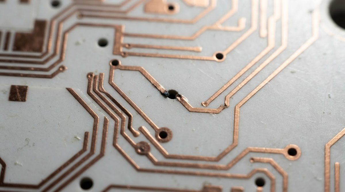
AOI is a machine-vision process. A camera (or array of cameras) captures high-resolution images of the board surface under controlled lighting. Software compares each captured image against a reference — either a golden board image or a CAD-derived model — and flags any pixel region that deviates beyond a set threshold.
On FR-4, the green solder mask provides strong contrast against copper traces and bare laminate. On a ceramic PCB, there is no solder mask in most designs. The contrast comes from metallization (copper, gold, silver, or tungsten) against the bare ceramic. Alumina (Al₂O₃) substrates are white to off-white; aluminum nitride (AlN) substrates range from grey to dark grey. These differences mean the AOI lighting recipe — the angle, wavelength, and intensity of illumination — must be tuned per substrate material and metallization type.
Most modern AOI systems use multi-angle, multi-wavelength LED illumination (red, green, blue, plus coaxial and angled rings). The operator builds an inspection program by teaching the system which colour-angle combination best separates metal from substrate, then sets thresholds for acceptable trace width, spacing, pad size, and edge roughness.
Defects That AOI Inspection Catches on Ceramic PCBs
| Defect type | AOI detectable? | Typical resolution needed | Notes |
|---|---|---|---|
| Open trace | Yes | ≥ 15 µm gap | High contrast against bare ceramic |
| Short / bridge | Yes | ≥ 15 µm bridge | Especially common in fine-line DPC |
| Trace-width violation | Yes | ± 5 µm measurement | Compared against CAD nominal |
| Missing pad or feature | Yes | — | Detected by pattern matching |
| Nick or notch in trace | Yes | ≥ 10 µm depth | Reduces current-carrying capacity |
| Foreign material / contamination | Partial | ≥ 25 µm particle | Depends on contrast with substrate |
| Registration shift | Yes | ± 10 µm | Layer-to-fiducial offset |
| Subsurface void (DBC bond) | No | — | Requires X-ray or SAM |
| Ceramic micro-crack | Rarely | — | Only if crack reaches surface and is wide enough |
| Copper peel initiation | No | — | Requires copper peel strength testing |
Typical values for commercially available AOI systems (Koh Young, CyberOptics, Omron). Confirm against your specific equipment’s specification sheet.
Why Ceramic Substrates Need Different AOI Inspection PCB Programming Than FR-4
Three factors make ceramic AOI programming more demanding than standard FR-4 inspection:
1. No solder mask layer. On FR-4, the solder mask defines pad openings and trace boundaries, giving the AOI clear edges to lock onto. On most ceramic PCBs, the metallization sits directly on the substrate. The AOI must distinguish metal edges purely by reflectance and colour, which requires tighter lighting control.
2. High substrate reflectance. White alumina reflects 80–90% of visible light. Under coaxial illumination, the substrate can appear almost as bright as the metal, collapsing contrast. Angled illumination (30°–45° ring lights) typically works better because the diffuse ceramic surface scatters light differently than the specular metal surface.
3. Metallization variety. A single ceramic PCB line may run thick-film silver, thin-film gold, DPC copper, and DBC copper. Each metallization has a different reflectance spectrum. The AOI inspection program often needs per-part-number lighting recipes rather than a single factory-wide setting.
Shops that skip this tuning step see false-call rates of 5–15%, which slows the line and erodes operator trust in the system. A properly tuned ceramic AOI program should hold false calls below 1–2% per IPC-A-610 Class 3 criteria.
Where AOI Fits in the Ceramic PCB Inspection Sequence
AOI inspection on a PCB is most effective as an in-process gate, not a final acceptance test. A typical sequence for a DPC or DBC ceramic board:
- Incoming substrate inspection — visual and dimensional check of blank ceramic.
- Post-metallization AOI — the primary AOI step, catching patterning defects before any further processing.
- Post-plating AOI (if applicable) — verifying plating coverage and uniformity after electroless nickel/gold or other finishes.
- Electrical test — continuity and isolation, catching defects AOI cannot see (subsurface shorts, high-resistance opens).
- Final visual / AOI — a second optical pass after singulation and cleaning.
For multilayer ceramic builds (HTCC or LTCC), AOI runs on each layer’s print before lamination. This is critical because defects buried between layers cannot be reworked after co-firing.
Use the tool below to see which test methods — including AOI — apply to your board’s specific defect risks and quality class.
AOI Inspection PCB Limitations: When You Need More Than Optics
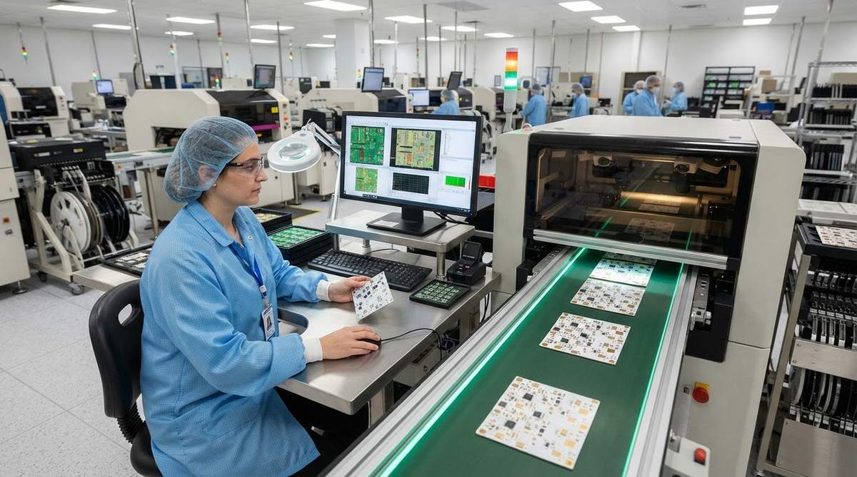
AOI sees surfaces. It cannot see through ceramic or metal. These defect categories require complementary methods:
- Subsurface voids and delamination — X-ray inspection or scanning acoustic microscopy (SAM).
- Electrical opens/shorts below detection resolution — flying-probe or bed-of-nails electrical test.
- Adhesion strength — destructive peel-strength testing per IPC-TM-650 2.4.8.
- Dielectric integrity — hipot / dielectric withstand testing at rated voltage.
- Ceramic body cracks — dye-penetrant inspection or high-frequency ultrasonic scanning for cracks that do not break the surface.
Relying on AOI alone for final acceptance is a common mistake in shops transitioning from FR-4 to ceramic. The defect mix is different. On FR-4, most defects are etching-related and surface-visible. On ceramic, bond-line voids, co-fire shrinkage errors, and substrate cracks account for a larger share of failures, and none of these show up under a camera.
When AOI Inspection Is Not the Right Tool for Your PCB
If your ceramic board has no surface metallization to inspect — for example, a bare substrate used as a heat spreader or spacer — AOI adds no value. Dimensional metrology (CMM or optical profilometry) is the correct inspection method.
For very low volumes (fewer than 10 pieces), the time spent programming the AOI system can exceed the time saved versus skilled manual inspection under a stereo microscope. AOI pays for itself on runs of roughly 25+ panels or on designs with feature sizes below 75 µm, where the human eye is unreliable.
For buried-layer defects in multilayer ceramic, AOI per layer before lamination helps, but post-lamination inspection requires X-ray or electrical test. AOI alone is insufficient for multilayer acceptance.
Frequently Asked Questions
Can AOI detect cracks in the ceramic substrate itself?
Only if the crack reaches the surface and is wide enough to create a visible contrast change — typically above 20–30 µm width. Hairline cracks and subsurface fractures are invisible to optical systems. Dye-penetrant or ultrasonic methods are needed for those.
Does AOI inspection replace electrical testing on a ceramic PCB?
No. AOI and electrical test catch different defect populations. AOI finds visual defects (nicks, contamination, registration errors) that may not cause an immediate electrical failure. Electrical test finds subsurface shorts, high-resistance opens, and isolation failures that AOI cannot see. Both are needed for Class 3 reliability.
How long does it take to program AOI for a new ceramic part number?
Expect 1–4 hours for initial programming and threshold tuning, depending on the complexity of the metallization pattern and the number of lighting recipes required. A simple single-layer DPC design on white alumina programs faster than a multi-metal thick-film design on dark AlN.
What AOI resolution do I need for ceramic PCBs with fine traces?
For trace/space down to 50 µm, a pixel resolution of 10–15 µm is standard. For trace/space of 75 µm and above, 20 µm resolution is adequate. The rule of thumb is that the pixel size should be no more than one-third of the smallest feature you need to measure.
Is 3D AOI better than 2D for ceramic boards?
3D AOI (which adds height measurement via structured light or phase-shift profilometry) is useful for inspecting solder paste deposits and component placement, but offers little advantage over 2D for bare metallization inspection on ceramic. The added cost and slower throughput of 3D systems are rarely justified unless you are also inspecting assembled boards on the same line.
Next Step
If you are specifying inspection requirements for a ceramic PCB project, review the full ceramic PCB testing and reliability screening overview to see how AOI fits alongside electrical, mechanical, and environmental tests. To discuss inspection coverage for your specific design, request a quote and note your quality requirements.