ENEPIG is a four-metal surface finish — electroless nickel / electroless palladium / immersion gold — that serves as a universal finish for ceramic PCBs requiring both soldering and wire bonding on the same board. The palladium interlayer (typically 0.05–0.30 µm) acts as a diffusion barrier that blocks the nickel-gold galvanic reaction responsible for black-pad defect, a failure mode that has ended many high-reliability programs using plain ENIG on ceramic substrates.
Key Takeaways
- ENEPIG deposits four layers on the copper pad: ~3–6 µm Ni, ~0.05–0.30 µm Pd, ~0.03–0.10 µm Au (per IPC-4556).
- The palladium barrier virtually eliminates black-pad defect, the primary reliability risk of ENIG.
- A single ENEPIG-finished board supports SMT soldering, gold wire bonding, and aluminum wedge bonding — no selective plating needed.
- ENEPIG adds roughly 15–30 % to finish cost compared with ENIG, driven mainly by the palladium bath.
- On ceramic substrates (Al₂O₃, AlN), adhesion of the electroless nickel to the metallisation layer is critical; DPC or thick-film copper must be clean and properly activated.
What Is ENEPIG and What Does Each Layer Do?
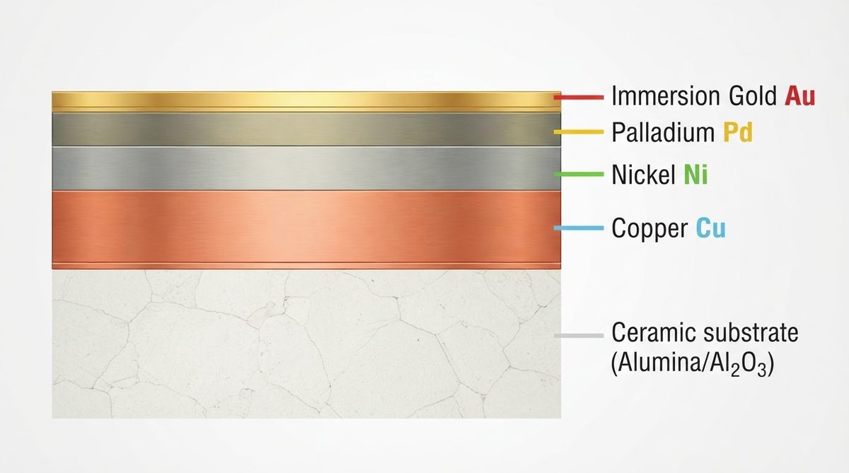
ENEPIG stands for Electroless Nickel / Electroless Palladium / Immersion Gold. The acronym describes the deposition order on top of the copper (or copper-alloy) pad. Each layer has a distinct engineering purpose.
| Layer | Typical thickness | Function | Source |
|---|---|---|---|
| Electroless Nickel (Ni-P) | 3–6 µm | Barrier to copper diffusion; solderable surface | IPC-4556 |
| Electroless Palladium | 0.05–0.30 µm | Blocks Ni–Au galvanic corrosion (black pad); wire-bondable | IPC-4556 |
| Immersion Gold | 0.03–0.10 µm | Oxidation protection for Pd; maintains shelf life and wettability | IPC-4556 |
Typical values per IPC-4556, for comparison only. Confirm against the datasheet for your specific grade.
The nickel layer carries the mechanical load during soldering and provides the diffusion barrier against copper migration. In ENIG, the thin immersion gold directly attacks the nickel surface during deposition, occasionally producing a hyper-corrosion (black-pad) layer at the Ni–Au interface. In ENEPIG, palladium deposits electrolessly onto the nickel first, sealing the surface before gold displacement begins. Because the gold displaces palladium rather than nickel, the corrosion mechanism that causes black pad is eliminated at its root.
ENEPIG Deposition on Ceramic Substrates
On FR-4, the copper foil is laminated and etched, leaving a relatively uniform surface for plating chemistry. Ceramic PCBs are different. The copper is applied by DPC (direct plated copper), thick-film printing, or DBC (direct bond copper), and each method produces a different surface morphology. ENEPIG chemistry must be tuned accordingly.
The general process sequence on a ceramic board is:
- Clean and micro-etch — remove oxides and organic residue from the copper trace surface. Ceramic areas must be masked or remain inert to the chemistry.
- Palladium activation — a thin catalytic Pd seed is deposited to initiate electroless nickel plating. (This activation step is separate from the Pd barrier layer.)
- Electroless nickel — Ni-P alloy (typically 7–10 wt% phosphorus for mid-phos) deposits at 80–90 °C for 20–30 minutes to reach 3–6 µm.
- Electroless palladium — Pd deposits from an amine-based or ammonia-based bath at 50–70 °C. Target is 0.05–0.30 µm.
- Immersion gold — Au displaces surface Pd atoms in a galvanic exchange at 80–90 °C. Target is 0.03–0.10 µm.
Adhesion of the nickel to the underlying copper on a ceramic substrate depends heavily on surface preparation. DPC copper is sputtered and electroplated, yielding a dense, smooth film. Thick-film copper is screen-printed and fired, producing a rougher, more porous surface with glass-frit binders. In both cases, the micro-etch step must be aggressive enough to expose fresh copper without undercutting fine traces. For ceramic PCB fabrication lines, this is one of the tightest process windows in the entire flow.
ENEPIG vs. ENIG on Ceramic PCBs
Most ceramic boards today ship with ENIG because it is well understood and less expensive. ENEPIG is justified when the application demands wire bonding, or when the reliability budget cannot tolerate any black-pad risk. The table below compares the two finishes head-to-head.
| Parameter | ENIG | ENEPIG | Unit / Condition |
|---|---|---|---|
| Layer count | 2 (Ni + Au) | 3 (Ni + Pd + Au) | — |
| Black-pad risk | Low but nonzero (IPC-4552 rev B improved) | Virtually zero | Per IPC-4556 |
| Gold wire bonding | Marginal — thin Au over Ni | Good — Pd/Au stack bonds reliably | MIL-STD-883 Method 2011 |
| Aluminum wedge bonding | Not recommended | Suitable | — |
| Solder joint strength (SAC305) | Good | Good to excellent | IPC J-STD-002 |
| Shelf life | 12+ months | 12+ months | Sealed, room temp |
| Relative finish cost | 1.0× | 1.15–1.30× | Typical for same board |
| Contact resistance | ~1–3 mΩ | ~1–3 mΩ | Per IPC-4552 / 4556 |
Typical values for commercially available finishes, for comparison only. Confirm against the datasheet for your specific grade.
If your ceramic board only needs SMT soldering and no wire bonding, ENIG is usually the more cost-effective choice. If the board carries both SMT components and wire-bonded die — common in power modules, RF hybrids, and LED packages — ENEPIG lets you run a single finish across all pads, eliminating the cost and risk of selective gold plating.
Use the tool below to compare ENEPIG against other ceramic PCB surface finishes side by side, including OSP coatings, immersion silver, and immersion tin.
[pcb_calc type=”surface-finish”]
Worked Example: Cost Impact of ENEPIG on a Power-Module Substrate
Consider a 50 × 50 mm Al₂O₃ 96 % DPC substrate with 60 % copper coverage. The finish area is approximately 1,500 mm². At typical bath loading, ENIG costs roughly $0.08–$0.12 per cm² of pad area, while ENEPIG runs $0.10–$0.15 per cm² due to the added palladium bath, longer process time, and tighter bath maintenance.
For this board: ENIG finish cost ≈ 15 cm² × $0.10 = $1.50. ENEPIG finish cost ≈ 15 cm² × $0.125 = $1.88. The delta is about $0.38 per unit — small in absolute terms, but it scales at volume. On a 10,000-unit run, that is $3,800. Whether that premium is justified depends on whether you need wire bonding or must guarantee zero black-pad rejects in a mission-critical application.
When NOT to Use ENEPIG
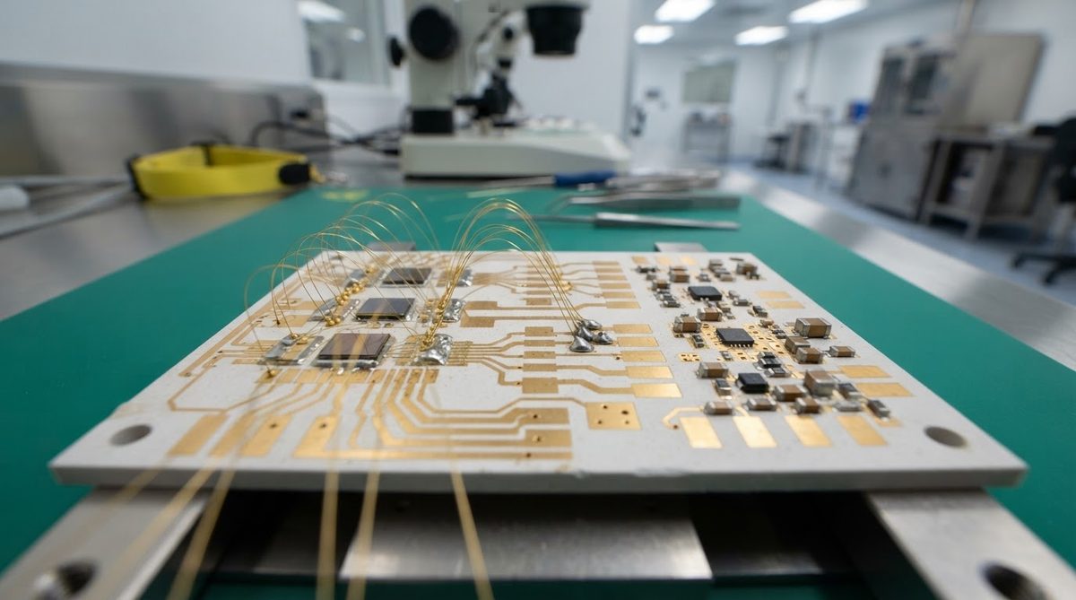
ENEPIG is not always the right answer. Skip it when:
- The board is solder-only with no wire bonding. ENIG or even a simpler ceramic PCB finish will perform identically at lower cost.
- Budget is the primary constraint. For prototyping or non-critical thermal substrates, OSP or immersion tin may suffice if shelf-life requirements are modest.
- You need heavy gold for repeated connector insertions. ENEPIG gold is only 0.03–0.10 µm — far too thin for edge connectors. Electrolytic hard gold (0.75+ µm) is the correct choice there.
- The substrate metallisation is incompatible. Some thin-film metallisation stacks (e.g., Ti/Pt/Au) already provide a bondable surface and do not benefit from an additional ENEPIG finish.
Reliability Considerations
Palladium dissolves into SAC305 solder during reflow, forming Pd-Sn intermetallics. At the thicknesses specified by IPC-4556 (≤ 0.30 µm), the amount of palladium entering the joint is small enough that it does not embrittle the solder. Studies published by Atotech and MacDermid Alpha show shear-strength retention above 95 % after 1,000 thermal cycles (−40 to +125 °C) for ENEPIG joints on alumina substrates. If palladium thickness creeps above 0.30 µm due to bath aging, the intermetallic volume increases and joint ductility can drop. Tight SPC on the palladium bath is non-negotiable.
For boards that will see ceramic-specific reflow profiles with peak temperatures above 260 °C, ENEPIG is well suited because neither nickel nor palladium oxidise significantly at those temperatures, preserving wettability through the entire profile.
Frequently Asked Questions
Can you wire bond directly to ENEPIG?
Yes. ENEPIG supports both gold ball bonding and aluminum wedge bonding. The palladium-gold surface provides a reliable bonding target per MIL-STD-883 Method 2011. Pull-strength results are typically comparable to electrolytic gold for gold wire, and superior to ENIG for aluminum wire.
Does ENEPIG add lead time compared with ENIG?
Expect 1–2 extra days in the plating step. The palladium bath runs at a slower deposition rate (typically 0.05–0.10 µm per 5–10 minutes), and the additional rinse and quality checks add cycle time. Total board lead time increase is usually minor relative to ceramic substrate fabrication itself.
Is ENEPIG compatible with lead-free and leaded solder?
ENEPIG works with both. SAC305, SnPb 63/37, and high-temperature AuSn (80/20) solders all wet reliably to the ENEPIG surface. The palladium layer dissolves into the solder during reflow, leaving a clean Ni-Sn intermetallic — the same joint metallurgy as ENIG.
How do I inspect ENEPIG thickness on a ceramic board?
X-ray fluorescence (XRF) is the standard non-destructive method. Measure nickel, palladium, and gold thickness at a minimum of three points per coupon per IPC-4556. On ceramic substrates, ensure the XRF calibration accounts for the non-metallic substrate backscatter, which differs from FR-4’s glass-epoxy.
Does ENEPIG affect high-frequency signal performance?
At frequencies below 10 GHz, the impact is negligible. Above 10 GHz, the nickel layer’s ferromagnetic properties can increase insertion loss on signal traces. If your design operates in the millimetre-wave range, consider immersion gold over sputtered copper (no nickel underlayer) or a thin-film gold finish instead.
Next Step
If your ceramic board needs both solder pads and wire-bond pads, request an ENEPIG quote with your Gerber files. Specify the palladium thickness range you need — standard (0.05–0.15 µm) or heavy (0.15–0.30 µm) — so the plating line can be set up correctly from the start. Upload your design files at AluminaPCB’s manufacturer selection guide to start the conversation.