Immersion gold on a ceramic PCB is almost always part of an ENIG (Electroless Nickel / Immersion Gold) stack: 3–6 µm of electroless nickel topped by 0.05–0.15 µm of gold, per IPC-4552 Rev. B. The gold protects the nickel from oxidation and provides a flat, solderable surface. On alumina or aluminum nitride substrates, ENIG is the most common finish for mixed-technology boards that need both SMT soldering and aluminum wire bonding.
Key Takeaways
- Standard ENIG gold thickness is 0.05–0.15 µm (2–6 µin) over 3–6 µm electroless Ni, per IPC-4552B.
- Shelf life exceeds 12 months when stored below 30 °C and 60% RH — far longer than OSP finishes on ceramic boards.
- Thicker gold (above ~0.10 µm) increases raw material cost roughly linearly, but the nickel bath chemistry and dwell time are the larger cost drivers.
- Gold embrittlement of solder joints is a real risk above approximately 3 wt% Au in the joint; keeping the immersion gold thin (≤0.15 µm) controls this.
- For heavy gold wire bonding, immersion gold alone is too thin — electrolytic or sputtered gold at 0.5–1.5 µm is required instead.
What Immersion Gold Actually Is
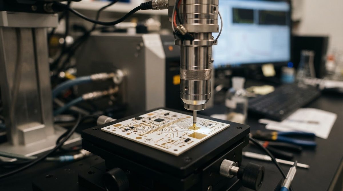
Immersion gold is a displacement reaction. Gold ions in solution displace nickel atoms at the surface, depositing a self-limiting layer typically 0.05–0.15 µm thick. Because the reaction stops once the nickel is fully covered, you cannot simply extend bath time to get thicker gold. This self-limiting behavior distinguishes immersion gold from electrolytic plating, where thickness is controlled by current and time.
On ceramic substrates the underlying conductor is usually thick-film or thin-film metallization — not etched copper foil. The electroless nickel step must nucleate on this metallization, which means the palladium activation chemistry and bath pH need tighter control than on FR-4 copper. Poorly activated thick-film conductors are the most common root cause of skip plating on ceramic ENIG.
Gold Thickness, Cost, and Embrittlement Trade-offs
Gold is expensive. At roughly $65–80 per troy ounce (mid-2024 spot), even a few microinches of extra thickness adds measurable cost on high-volume panels. But the real trade-off is functional: too little gold and the nickel oxidizes before assembly; too much gold and the solder joint becomes brittle.
Gold embrittlement occurs when dissolved gold in a tin-based solder joint exceeds about 3 wt%. For a standard ENIG layer of 0.05–0.10 µm Au, the gold contribution to a BGA or QFN joint is well below that threshold. Push above 0.15 µm — or reflow the same pad multiple times — and you approach the danger zone. IPC-J-STD-001 Section 5 addresses this indirectly through visual inspection criteria for brittle fracture.
Use the calculator below to estimate how gold thickness and panel area affect your finish cost per board. Enter your substrate dimensions, gold thickness target, and batch size.
[pcb_calc type=”gold-thickness-cost”]
ENIG Spec Table for Ceramic Substrates
| Parameter | Value | Unit | Condition | Source |
|---|---|---|---|---|
| Gold thickness | 0.05–0.15 | µm | As deposited, XRF measurement | IPC-4552B |
| Nickel thickness | 3–6 | µm | As deposited | IPC-4552B |
| Nickel phosphorus content | 7–12 | wt% | Mid-phosphorus bath | IPC-4552B |
| Surface roughness (Ra) | 0.1–0.3 | µm | After gold deposition | Typical, process-dependent |
| Shelf life | >12 | months | <30 °C, <60% RH, sealed | IPC-4552B |
| Solder wetting angle (SAC305) | <30 | degrees | Fresh surface, reflow | IPC J-STD-003C |
| Contact resistance | <20 | mΩ | 1 mm² pad, 100 g force | Typical measurement |
Typical values for commercially available material, for comparison only. Confirm against the datasheet for your specific grade.
Immersion Gold vs. Other Finishes on Ceramic
ENIG is not the only option. The table below compares it with the finishes most commonly applied to ceramic substrates.
| Parameter | ENIG | Immersion Silver | Immersion Tin | Electrolytic Au |
|---|---|---|---|---|
| Typical thickness (Au/Ag/Sn) | 0.05–0.15 µm | 0.15–0.40 µm | 0.8–1.5 µm | 0.5–2.5 µm |
| Shelf life | >12 months | 6–9 months | 3–6 months | >12 months |
| Wire bondable (Au wire) | No (too thin) | No | No | Yes |
| Wire bondable (Al wire) | Marginal | No | No | Yes |
| Relative cost | Medium | Low–Medium | Low | High |
| Coplanarity | Excellent | Good | Good | Excellent |
| Gold embrittlement risk | Low if ≤0.15 µm | None | None | High if thick |
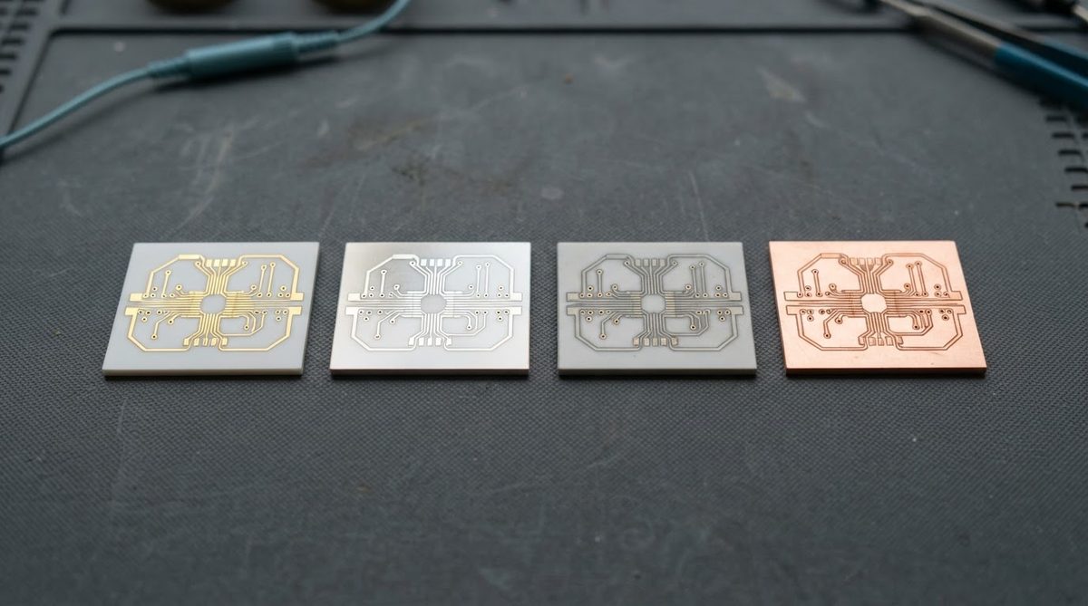
For boards that need only SMT soldering and long shelf life, ENIG hits the sweet spot. If your design requires gold wire bonding at 25 µm diameter, look at gold-metallized ceramic substrates with electrolytic or sputtered gold instead. For cost-sensitive RF boards with short storage windows, immersion silver for ceramic PCBs may be a better fit.
Worked Example: Gold Contribution to Solder Joint
Suppose you have a 0.5 mm pitch QFN pad, 0.25 × 0.50 mm, with ENIG at 0.10 µm Au. The gold volume per pad is approximately 0.25 × 0.50 × 0.0001 mm = 1.25 × 10⁻⁵ mm³. Gold density is 19.3 g/cm³, so the gold mass per pad is about 0.24 µg. A typical solder paste deposit on that pad is roughly 0.08 mm³ of SAC305 (density ~7.4 g/cm³), giving ~590 µg of solder. The gold concentration in the joint: 0.24 / 590 ≈ 0.04 wt% — well below the 3 wt% embrittlement threshold. Even after three reflow cycles, the dissolved gold remains negligible at standard ENIG thickness.
Process Considerations on Ceramic Substrates
Ceramic substrates present two challenges that organic boards do not. First, the metallization adhesion layer (often a TiW or Cr sputter layer, or a thick-film glass frit bond) must survive the acidic nickel and gold baths without delamination. Second, ceramic is chemically inert, so any exposed substrate surface between pads will not react — but bath chemistry can wick under poorly defined metallization edges, causing undercutting.
Rinsing is also more critical. Ceramic’s low porosity means trapped chemistry is rare, but thick-film surfaces can have micro-porosity that traps chloride or phosphate ions. Thorough DI water rinsing and a final hot-air dry step prevent corrosion under the gold layer. For guidance on soldering profiles after ENIG application, see reflow profiles for ceramic PCBs.
When Not to Use Immersion Gold on Ceramic
Gold wire bonding: ENIG gold at 0.05–0.15 µm is too thin for reliable thermosonic gold wire bonding. You need electrolytic gold at 0.5 µm minimum, often 1.0–1.5 µm.
Ultra-high-frequency RF: The nickel underlayer in ENIG is ferromagnetic and introduces loss above roughly 10 GHz. For millimeter-wave ceramic boards, consider immersion silver or direct gold metallization without a nickel barrier.
Budget-constrained, short-life products: If boards ship to assembly within weeks and the product life is under five years, immersion tin on ceramic costs less and solders well. The shorter shelf life is irrelevant if your supply chain is fast.
Boards with no soldering: If the ceramic substrate is used purely as a thermal carrier with die-attach epoxy and no solder, bare metallization or a simple organic coat may suffice.
Frequently Asked Questions
Can I wire-bond directly to immersion gold on a ceramic PCB?
Aluminum wedge bonding to ENIG is possible but marginal — the thin gold wears through to nickel during ultrasonic scrub. Gold ball bonding requires at least 0.5 µm of gold, which immersion chemistry cannot reach. Use electrolytic or sputtered gold for reliable wire bonding.
Does ENIG add measurable thermal resistance to a ceramic substrate?
No. The combined nickel-gold layer is 3–6 µm thick. Even nickel’s moderate thermal conductivity (~90 W/mK) at that thickness contributes less than 0.001 °C/W to the total thermal path. The ceramic substrate itself dominates.
How do I verify immersion gold thickness after plating?
XRF (X-ray fluorescence) is the standard method, per IPC-4552B. Measure at a minimum of five points per panel. Acceptable gold thickness is 0.05–0.15 µm; nickel is 3.0–6.0 µm. Cross-sectional SEM provides a secondary check if XRF readings are borderline.
Will immersion gold survive multiple reflow cycles?
Yes. ENIG routinely withstands three or more lead-free reflow cycles (peak 260 °C) without measurable degradation of solderability. The gold dissolves into the solder during the first reflow, exposing the nickel-tin intermetallic that provides the actual metallurgical bond. Subsequent reflows act on this intermetallic, not on fresh gold.
Is ENIG RoHS compliant?
Yes. ENIG contains no lead, cadmium, mercury, or other restricted substances under RoHS Directive 2011/65/EU. The nickel and gold layers are both RoHS-compliant by composition.
Next Step
If you are specifying ENIG for a ceramic board, confirm your gold thickness requirement against your assembly process — SMT-only versus mixed wire-bond. Review the full range of options on the ceramic PCB surface finish overview, then request a quote with your Gerber files and finish callout to get exact pricing for your panel size and volume.