Immersion tin deposits a thin, dense layer of pure tin (typically 0.8–1.2 µm) directly onto exposed copper on a ceramic PCB through a chemical displacement reaction. It delivers excellent coplanarity for fine-pitch components, costs less than ENIG or immersion silver, and is fully lead-free. The trade-off: a shelf life of roughly 6 months before solderability degrades, plus a non-zero risk of tin whisker growth in high-reliability environments.
Key Takeaways
- Immersion tin deposit thickness is typically 0.8–1.2 µm per IPC-4554, providing a flat, solderable surface suitable for fine-pitch QFP and BGA pads.
- Shelf life before reflow is limited to approximately 6 months when boards are vacuum-sealed with desiccant; exposed boards degrade faster.
- Tin whisker growth is a documented reliability concern, especially above 50 °C and in high-humidity environments, per JEDEC JESD201.
- Immersion tin costs roughly 30–50 % less per panel than ENIG on the same ceramic substrate, making it attractive for cost-sensitive, high-volume runs.
- The finish is not recommended for press-fit connectors, multiple reflow cycles, or applications requiring >12 months of storage before assembly.
What Is Immersion Tin and How Does It Work on Ceramic?
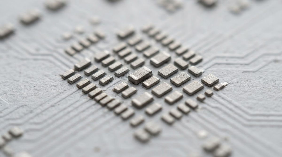
Immersion tin is a chemical displacement process. The ceramic board, with its patterned copper (applied by DPC, thick-film, or plating), is immersed in an acidic tin bath. Copper atoms at the surface dissolve into solution while tin ions deposit in their place. The reaction is self-limiting: once a continuous tin layer covers all exposed copper, deposition slows and eventually stops. This yields a uniform coating thickness regardless of pad geometry—an advantage over electrolytic processes that plate thicker at edges.
On ceramic substrates such as 96 % alumina or aluminum nitride, the process is identical in chemistry to FR-4 but demands tighter process control. Ceramic boards are more brittle, so handling fixtures must avoid point loading. The substrate itself is chemically inert and unaffected by the tin bath, which means only the copper traces and pads receive the deposit. Adhesion between copper and the ceramic (governed by the metallization process, not the surface finish) must already be sound before immersion tin is applied.
Immersion Tin Specifications and Typical Properties
| Parameter | Value | Unit | Condition | Source |
|---|---|---|---|---|
| Tin thickness | 0.8–1.2 | µm | As deposited | IPC-4554 |
| Tin purity | ≥ 99.0 | % | — | IPC-4554 |
| Surface roughness (Ra) | 0.3–0.8 | µm | Depends on underlying Cu | Typical industry data |
| Contact angle (solder wetting) | < 30 | ° | SAC305, fresh deposit | IPC J-STD-002 |
| Shelf life (vacuum-sealed) | ~6 | months | 25 °C, < 30 % RH | Industry consensus |
| Max reflow cycles | 1–2 | — | SAC305, peak 245 °C | Process guideline |
| RoHS compliant | Yes | — | Lead-free Sn | EU 2015/863 |
Typical values for commercially available material, for comparison only. Confirm against the datasheet for your specific grade.
Immersion Tin vs. Other Ceramic PCB Finishes
Choosing a surface finish on ceramic always involves balancing cost, shelf life, solderability, and long-term reliability. Below is a head-to-head comparison against the finishes most commonly applied to ceramic substrates.
| Parameter | Immersion Tin | ENIG | Immersion Silver | OSP |
|---|---|---|---|---|
| Typical thickness | 0.8–1.2 µm Sn | 3–5 µm Ni + 0.05–0.1 µm Au | 0.15–0.40 µm Ag | 0.2–0.5 µm organic |
| Coplanarity | Excellent | Excellent | Excellent | Good |
| Shelf life | ~6 months | 12+ months | ~6 months (tarnish risk) | ~3 months |
| Max reflow passes | 1–2 | 3–6 | 2–3 | 1–2 |
| Wire bondable | No | Au wire: yes | Limited | No |
| Whisker risk | Yes | No | No | No |
| Relative cost (per panel) | 1× | 2.0–2.5× | 1.3–1.6× | 0.7–0.9× |
Relative costs are approximate and vary with panel size, pad density, and supplier. Values based on typical ceramic PCB production lots.
For a broader overview of all available options, see ceramic PCB surface finish options. If your design can tolerate a shorter shelf life and single reflow, OSP finish on ceramic boards costs even less but offers no metallic protection.
Cost Comparison of Ceramic PCB Surface Finishes
Enter your board dimensions and pad count below to see an estimated cost difference between immersion tin, ENIG, immersion silver, and OSP on a ceramic substrate.
[pcb_calc type=”finish-cost”]
The calculator above uses typical bath chemistry costs and processing times. Actual quotes will vary with order volume and substrate material.
Tin Whisker Risk: What You Need to Know
Tin whiskers are conductive, crystalline filaments that can grow spontaneously from pure tin surfaces. They range from a few micrometres to several millimetres in length and can bridge adjacent conductors, causing short circuits. JEDEC standard JESD201 defines acceptance test methods for tin whisker susceptibility.
On ceramic PCBs, the risk is modulated by several factors. Compressive stress in the tin layer (from copper-tin intermetallic growth) is the primary driver. Elevated temperature and humidity accelerate whisker nucleation. For consumer electronics with a 3–5 year service life, the risk is generally acceptable. For aerospace, medical implants, or high-reliability military electronics, most specifications prohibit pure tin finishes entirely. If your product falls under aerospace and defense reliability requirements, choose ENIG or electrolytic nickel-gold instead.
Mitigation Strategies
If immersion tin is otherwise the best fit for your project, several mitigation steps reduce whisker risk:
- Reflow solder within 30 days of board receipt. The solder joint consumes the tin layer, eliminating the whisker-prone surface.
- Specify conformal coating (acrylic or urethane, ≥ 25 µm) over all exposed tin after assembly. This does not prevent whisker growth but contains whiskers mechanically.
- Store boards vacuum-sealed with desiccant at < 25 °C and < 30 % RH until assembly.
- Anneal the tin deposit at 150 °C for 1 hour within 24 hours of plating. This relieves compressive stress and slows intermetallic growth, per NASA-STD-6012 guidance.
Reflow Soldering Immersion Tin on Ceramic
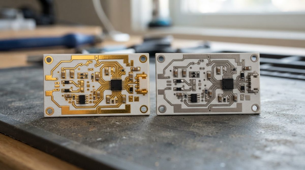
Immersion tin is consumed during reflow. The tin layer alloys with the solder paste to form a Cu-Sn intermetallic bond. For SAC305 solder at a peak reflow temperature of 240–250 °C, the entire 1 µm tin deposit is consumed in a single pass. A second reflow is possible if the first pass left sufficient wettable area, but solder joint quality degrades noticeably by the third pass.
Ceramic substrates have near-zero CTE (6–8 ppm/°C for alumina vs. 17 ppm/°C for copper), so thermal shock during reflow can stress solder joints differently than on FR-4. Follow ceramic-specific reflow profile guidelines to manage ramp rates and avoid cracking the substrate.
When Not to Use Immersion Tin on Ceramic
Immersion tin is the wrong finish in these situations:
- Long storage before assembly. If boards will sit in inventory for more than 6 months, ENIG or electrolytic gold is a better choice.
- Multiple reflow cycles. Double-sided reflow or rework-intensive assemblies need a finish that survives 3+ thermal excursions. ENIG handles this well.
- Wire bonding. Tin is not wire-bondable. Use ENIG (Au wire) or electrolytic gold (Au or Al wire).
- High-reliability / long-life products. Aerospace, implantable medical, and military programs often prohibit pure tin per GEIA-STD-0005-2 or equivalent. Choose a tin-free finish.
- Press-fit connectors. The thin tin layer is easily damaged by mechanical insertion. ENIG or hard gold plating is standard for press-fit zones.
- Harsh-environment exposure. Sulfur-rich or high-humidity atmospheres accelerate tin oxidation and whisker growth. Immersion silver on ceramic or ENIG performs better in corrosive environments, though silver has its own tarnish concerns.
Worked Example: Finish Selection for a Sensor Module
Consider a 25 × 25 mm alumina (96 %) substrate carrying a MEMS pressure sensor in a BGA-16 package. The assembly sees a single reflow, ships within 60 days of board fabrication, and operates in a sealed enclosure at 25–60 °C for a 5-year service life.
Immersion tin is a good fit here. The single reflow consumes the tin layer, eliminating long-term whisker risk. The 60-day ship window is well within the 6-month shelf life. Fine-pitch BGA pads benefit from the excellent coplanarity of immersion tin. And the cost saving of 30–50 % over ENIG matters when producing 10 000+ units per year.
If the same sensor module were destined for a satellite with a 15-year mission life and no conformal coating, immersion tin would be disqualified on whisker risk alone. ENIG would be the default, despite the cost premium.
Frequently Asked Questions
Does immersion tin work on aluminum nitride (AlN) substrates?
Yes. The tin displacement reaction occurs on the copper metallization, not on the ceramic itself. As long as the AlN substrate has properly adhered copper traces (via DPC, DBC, or sputtering), immersion tin deposits normally. The ceramic material is chemically inert to the tin bath.
Can I rework a ceramic PCB with an immersion tin finish?
Rework is possible but limited. The original tin layer is consumed during the first reflow, so the rework site exposes bare copper-tin intermetallic. Flux and fresh solder paste can wet this surface, but joint reliability is reduced. For boards that may need rework, ENIG is a safer choice. See the full guide on reworking ceramic PCBs for technique details.
How do I store immersion tin ceramic boards before assembly?
Vacuum-seal each panel or individual board with desiccant immediately after the finish is applied. Store at ≤ 25 °C and ≤ 30 % RH. Under these conditions, solderability is maintained for approximately 6 months. Once the vacuum seal is broken, use the boards within 24–48 hours for best results.
Is immersion tin compatible with lead-free solder paste?
Yes. Immersion tin is specifically designed for lead-free assembly. SAC305, SAC387, and other Sn-Ag-Cu alloys wet immersion tin surfaces readily, with contact angles typically below 30° per IPC J-STD-002 testing. Tin-lead (SnPb) solder also works, though the finish itself is lead-free and RoHS-compliant.
What happens if I exceed the shelf life?
Tin oxidation increases and copper-tin intermetallic growth reduces the available pure tin for wetting. Solderability testing per IPC J-STD-002 will show higher contact angles and incomplete wetting. Boards stored beyond 6 months should be tested before committing to production assembly. Stripping and re-plating is sometimes possible but adds cost and risks damaging fine traces.
Next Step
If immersion tin fits your project requirements, request a quote with your Gerber files and specify “immersion tin” as the surface finish. For help deciding between finishes, the ceramic PCB FAQ covers common selection questions. You can also upload your design files directly for a fast turnaround on pricing and lead time.