Aluminum nitride (AlN) ceramic PCBs are widely used in semiconductor packaging because AlN combines high thermal conductivity (170–230 W/mK at 25 °C, per Kyocera SH-30 and Maruwa AN series datasheets) with a coefficient of thermal expansion (CTE) of 4.4–4.7 ppm/°C—close to silicon (2.6 ppm/°C) and GaN (3.2 ppm/°C). That CTE proximity reduces solder-joint fatigue and die cracking under thermal cycling, which is the primary reason packaging engineers choose a semiconductor packaging AlN PCB over alumina or metal-core alternatives.
Key Takeaways
- AlN thermal conductivity is 170–230 W/mK at 25 °C, roughly 6–8× higher than 96% alumina (24–28 W/mK).
- AlN CTE of 4.4–4.7 ppm/°C closely matches Si (2.6 ppm/°C) and GaN (3.2 ppm/°C), reducing thermomechanical stress on die-attach joints.
- Common metallization routes for semiconductor packaging AlN PCB substrates are DBC (direct bond copper), AMB (active metal brazing), and thin-film sputtering.
- AlN substrates cost 3–5× more per unit area than 96% alumina; the premium is justified only when thermal or CTE requirements rule out cheaper options.
- AlN is hygroscopic: unprotected surfaces degrade in humid environments, requiring passivation or hermetic sealing in many packages.
Why Semiconductor Packaging AlN PCB Substrates Dominate High-Power Applications
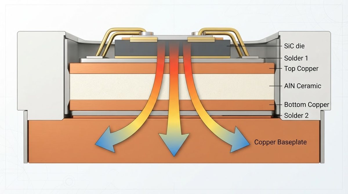
Power semiconductors—SiC MOSFETs, GaN HEMTs, high-power laser diodes, and IGBT modules—dissipate tens to hundreds of watts per square centimeter. The substrate between the die and the heat sink must conduct that heat out quickly while surviving thousands of thermal cycles between –55 °C and +175 °C (or higher for SiC gate drivers). Two properties dominate the selection: thermal conductivity and CTE match to the die material.
A CTE mismatch of more than ~3 ppm/°C between die and substrate introduces shear stress in the solder or sinter layer during every temperature swing. Over 1 000 cycles at ΔT = 200 °C, that stress nucleates cracks that raise thermal resistance and eventually cause field failure. AlN’s 4.4–4.7 ppm/°C sits between silicon and copper (17 ppm/°C), giving a mismatch to Si of only ~2 ppm/°C. By comparison, 96% alumina at 7.1 ppm/°C and copper MCPCB at 17 ppm/°C both impose significantly higher stress on the die attach.
AlN Properties Compared to Other Packaging Substrates
| Parameter | AlN | Al₂O₃ 96% | Al₂O₃ 99.6% | Si₃N₄ | Unit | Condition |
|---|---|---|---|---|---|---|
| Thermal conductivity | 170–230 | 24–28 | 28–35 | 70–90 | W/mK | 25 °C, ASTM E1461 |
| CTE | 4.4–4.7 | 7.0–7.2 | 7.0–7.2 | 2.5–3.3 | ppm/°C | 25–400 °C |
| Flexural strength | 300–400 | 300–380 | 380–450 | 650–900 | MPa | ASTM C1161, 3-pt bend |
| Dielectric strength | 14–17 | 10–15 | 12–16 | 12–18 | kV/mm | 25 °C, IEC 60672 |
| Relative cost (per cm²) | 3–5× | 1× (baseline) | 1.5–2× | 4–6× | — | Typical volume pricing |
Typical values for commercially available material, for comparison only. Confirm against the datasheet for your specific grade. Sources: Kyocera SH-30 datasheet, Maruwa AN-200 datasheet, CoorsTek ADS-996 datasheet.
Si₃N₄ offers superior mechanical toughness and an even closer CTE to silicon, but it is more expensive and harder to metallize than AlN. For most semiconductor packaging AlN PCB applications where thermal conductivity is the primary driver, AlN wins on performance-per-dollar. For applications demanding extreme mechanical reliability under vibration—such as AlN substrates in aerospace and defense—Si₃N₄ may be worth evaluating alongside AlN.
Metallization Options for Semiconductor Packaging AlN PCB Substrates
The metallization method determines the current-carrying capacity, die-attach compatibility, and thermal cycle reliability of the finished package substrate.
DBC (Direct Bond Copper)
Copper foil is bonded to AlN through a thin copper-oxide eutectic layer at ~1 065 °C. DBC on AlN delivers copper thicknesses of 0.15–0.5 mm and is the workhorse for power modules. One limitation: the bond relies on an oxide interface, and AlN does not form a native oxide as readily as alumina. Most DBC-on-AlN processes use a pre-oxidation step or a thin alumina interlayer, adding cost and process complexity.
AMB (Active Metal Brazing)
A titanium-containing braze alloy (typically AgCuTi) wets the AlN surface directly, creating a strong chemical bond without pre-oxidation. AMB supports copper thicknesses up to 0.8 mm and delivers better thermal-cycle performance than DBC on AlN, per published data from Infineon and Heraeus (Infineon AN2019-03). AMB is increasingly the default for SiC power modules rated above 200 A.
Thin-Film Sputtering
For RF and optoelectronic packages requiring fine features (trace/space below 50 µm), sputtered Ti/Pt/Au or Ti/Ni/Au metallization on AlN provides the necessary resolution. Thin-film AlN substrates are standard in laser-diode submounts and MMIC carrier packages. Learn more about ceramic PCB fabrication capabilities including thin-film processing.
Worked Example: Thermal Resistance of an AlN Packaging Substrate
Consider a SiC MOSFET die (4 mm × 4 mm) dissipating 80 W, mounted on a 0.635 mm thick AlN substrate with thermal conductivity of 180 W/mK.
Conduction thermal resistance through the substrate:
Rth = t / (k × A) = 0.000635 m / (180 W/mK × 0.000016 m²) = 0.22 °C/W
Temperature rise across the substrate alone: ΔT = 80 W × 0.22 °C/W = 17.6 °C.
If the same geometry used 96% alumina (k = 26 W/mK): Rth = 0.000635 / (26 × 0.000016) = 1.53 °C/W, giving ΔT = 122 °C. That 100 °C difference is the reason AlN dominates high-power semiconductor packaging.
Enter your own substrate dimensions, material, and power dissipation below to estimate junction-to-case temperature rise for your semiconductor packaging AlN PCB design.
Design Considerations for AlN in Semiconductor Packages
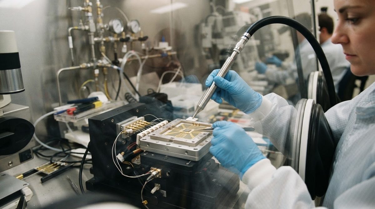
Hygroscopic degradation. AlN reacts with moisture to form aluminum hydroxide, which roughens the surface and degrades thermal performance over time. Packages must be hermetically sealed, or the AlN surface must be passivated (commonly with a thin SiO₂ or Al₂O₃ layer). This is a real failure mode, not a theoretical concern—unprotected AlN substrates stored in >60% RH environments show measurable surface degradation within weeks.
Die-attach selection. AuSn solder (80Au/20Sn, Tm = 280 °C) and silver sintering are the two most common die-attach methods for ceramic substrates. Silver sintering offers lower thermal resistance (Rth < 0.01 °C/W for a 4 × 4 mm die) and survives higher operating temperatures than AuSn, but requires specific surface metallization (Ag or Au finish) and sintering pressure of 10–30 MPa.
Via and cavity design. AlN substrates can be laser-drilled for thermal or electrical vias, but the minimum practical via diameter is ~100 µm, and via metallization adds process steps. Cavity packages for laser diodes or MEMS sensors require co-fired or machined AlN, increasing lead time and cost.
Typical Applications for Semiconductor Packaging AlN PCBs
- SiC and GaN power modules — half-bridge and full-bridge configurations for EV inverters and industrial drives. AlN substrates in automotive electronics must meet AEC-Q200 and IATF 16949 quality standards.
- High-power laser diode submounts — AlN’s CTE match to GaAs (5.7 ppm/°C) and InP (4.6 ppm/°C) makes it the standard submount material for telecom and industrial laser bars.
- UV and UV-C LED packages — AlN reflects UV wavelengths better than alumina and handles the concentrated heat flux of high-power UV dies. See AlN PCBs for UV LED applications for detail.
- MMIC and RF module carriers — thin-film AlN substrates carry GaN MMIC dies in radar and 5G front-end modules.
When Not to Use AlN for Semiconductor Packaging
Low-power packages (< 5 W). If the die dissipates modest power and the CTE mismatch to alumina is tolerable, 96% alumina substrates cost 3–5× less and are easier to source. Most standard LED and sensor packages fall into this category.
High-vibration, high-shock environments without hermetic sealing. AlN’s flexural strength (300–400 MPa) is adequate for most packages, but Si₃N₄ (650–900 MPa) is a better choice when the substrate must survive repeated mechanical shock or when a thinner substrate is needed to save weight.
Cost-sensitive consumer products. If the product’s thermal budget can be met with an aluminum MCPCB or a thick-copper FR-4 build, the AlN premium is not justified.
Humid, non-sealed environments. Unless the AlN surface is passivated or the package is hermetically sealed, moisture degradation will limit service life.
Frequently Asked Questions
Is AlN compatible with lead-free solder reflow?
Yes. AlN substrates with DBC or AMB copper metallization survive standard SAC305 reflow profiles (peak 250–260 °C). The substrate itself is rated well above 300 °C. Ensure the surface finish (ENIG, ENEPIG, or bare Au) is compatible with your specific solder alloy.
How does AlN compare to BeO for semiconductor packaging?
BeO offers slightly higher thermal conductivity (250–300 W/mK) than AlN, but beryllium oxide dust is a confirmed human carcinogen that causes chronic beryllium disease. Regulatory restrictions (OSHA PEL: 0.2 µg/m³) and disposal costs have driven most packaging applications to AlN. BeO is now used only where no alternative meets the thermal requirement and full hazard controls are in place.
Can I get AlN substrates with plated through-holes?
Yes, but the process is more complex and costly than for alumina. Vias are typically laser-drilled and filled with tungsten paste (co-fired) or plated copper (post-fired). Minimum via diameter is around 100 µm for laser drilling. Discuss via requirements early in design to avoid surprises in lead time.
What is the maximum continuous operating temperature for an AlN substrate?
The AlN ceramic itself is stable above 1 000 °C in inert atmosphere. The practical limit is set by the metallization and solder: DBC copper is reliable to ~400 °C, AMB to ~500 °C, and AuSn die attach to ~280 °C. Silver-sintered joints push the operating ceiling to ~300 °C continuously.
Does AlN need special handling during assembly?
AlN substrates are brittle (fracture toughness ~2.5 MPa·m½) and hygroscopic. Store them in dry, vacuum-sealed packaging until use. Handle with gloves and vacuum wands—finger oils accelerate surface degradation. Use matched-CTE tooling during reflow to prevent warping.
Next Step
If your package design requires AlN substrates, start by defining the die size, power dissipation, and thermal-cycle profile. These three parameters determine whether DBC, AMB, or thin-film metallization is the right route. You can request a quote with your specific substrate dimensions and metallization requirements through our AlN ceramic PCB manufacturing page.