Ceramic PCB manufacturing bonds conductive traces to a ceramic substrate using one of five main processes: DPC (Direct Plated Copper), DBC (Direct Bonded Copper), AMB (Active Metal Brazing), HTCC (High-Temperature Co-fired Ceramic), or LTCC (Low-Temperature Co-fired Ceramic). Each process dictates the minimum trace width, copper thickness, substrate material, and thermal performance you can achieve. This article walks through every major step so you can match the right process to your board.
Key Takeaways
- DPC delivers the finest traces (down to 20–50 µm line/space) and is the go-to process for high-density ceramic circuits on Al₂O₃ or AlN.
- DBC bonds thick copper foil (typically 0.127–0.635 mm) directly to alumina or AlN at ~1065 °C, making it the standard for power modules above 50 A.
- AMB uses a Ti/Ag/Cu braze alloy at ~850 °C to bond copper to Si₃N₄ or AlN, achieving the highest thermal-cycle reliability for EV and traction inverters.
- HTCC fires at 1500–1600 °C with tungsten or moly metallization, producing hermetic multilayer ceramic PCBs used in military and aerospace packaging.
- LTCC fires at 850–900 °C and allows silver or gold conductors, supporting embedded passives and RF structures up to mmWave frequencies.
How Ceramic PCB Manufacturing Differs from FR-4
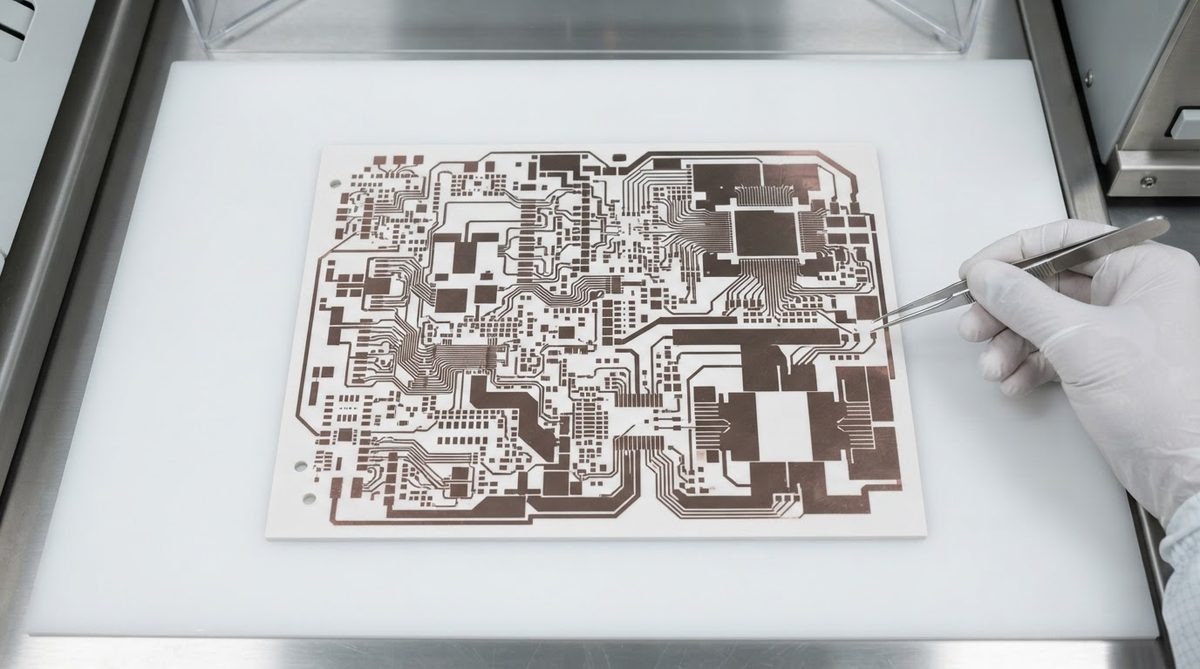
FR-4 fabrication starts with a copper-clad laminate. You etch away copper you don’t need. Ceramic PCB manufacturing starts with a bare, fired ceramic substrate and adds metal to it. That inversion changes almost everything: the equipment, the chemistry, the tolerances, and the cost.
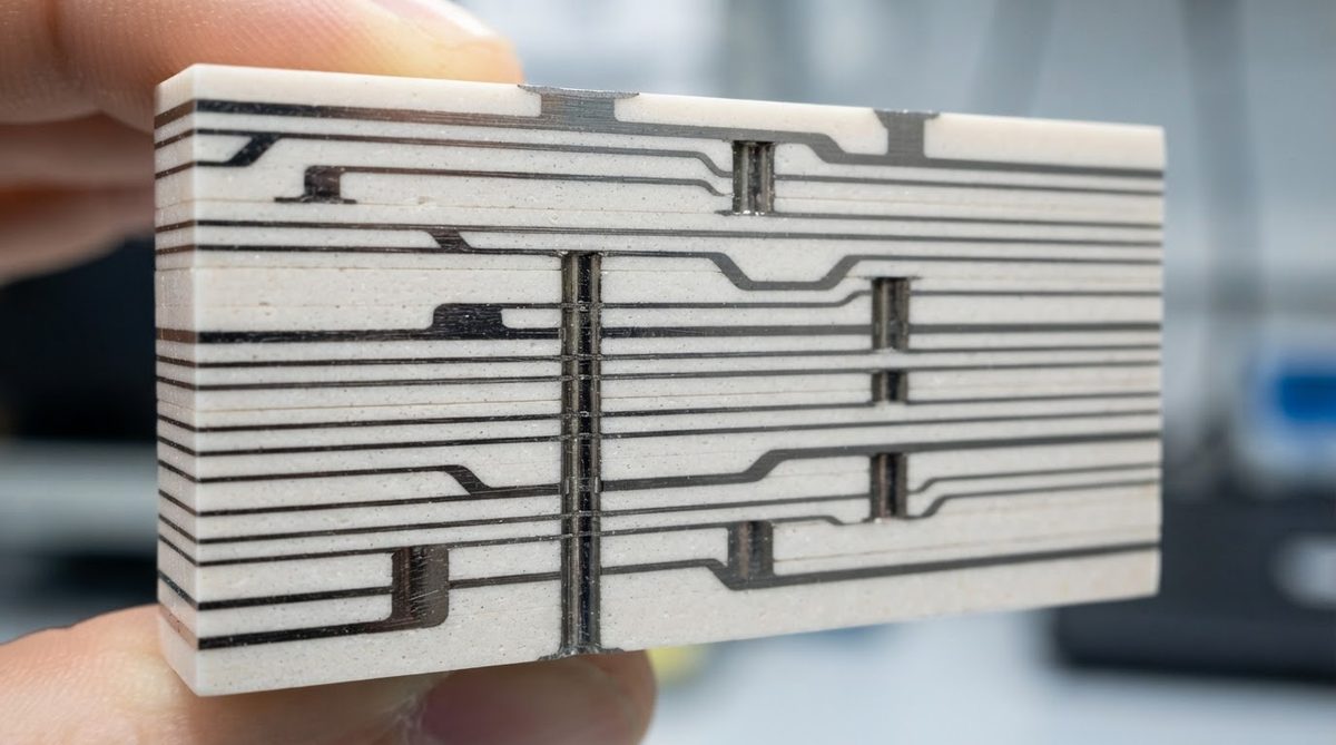
Ceramic substrates arrive pre-sintered (in DPC, DBC, and AMB processes) or as unfired “green tape” (in HTCC and LTCC). There is no drilling-and-plating via process in the FR-4 sense. Vias in co-fired ceramics are punched or laser-cut before firing and filled with conductive paste. Vias in post-fired substrates are either laser-drilled and plated or achieved through metallized through-holes. For a broader comparison of the full PCB manufacturing process from Gerber to finished board, see our pillar guide.
The Five Core Ceramic PCB Manufacturing Processes
DPC — Direct Plated Copper
DPC is a thin-film metallization process. A sputtering system deposits a seed layer (typically Ti/Cu or Cr/Cu, 0.1–0.3 µm) onto a polished ceramic substrate. Photoresist is applied, exposed, and developed to define the circuit pattern. Copper is then electroplated to the target thickness, usually 1–70 µm. After stripping the resist, the seed layer is etched away between traces.
DPC achieves the finest resolution of any ceramic metallization method. Line/space of 20–50 µm is routine; some facilities push below 20 µm. Because the copper is deposited directly onto the ceramic with a sputtered adhesion layer, bond strength is high (typically ≥6 MPa peel) and the copper–ceramic interface is void-free. DPC is the dominant process for LED submounts, sensor substrates, RF hybrid circuits, and AlN substrates used in semiconductor packaging.
Limitations: copper thickness is capped around 70 µm in most DPC lines. If you need 300 µm copper for high-current busbars, DPC is not the process. Substrate surface finish matters; Ra ≤ 0.3 µm is typical for reliable seed adhesion, which means polished-grade substrates cost more.
DBC — Direct Bonded Copper
DBC bonds a sheet of oxygen-free copper foil to a ceramic substrate at approximately 1065 °C in a nitrogen atmosphere containing trace oxygen. At this temperature, a thin Cu–O eutectic liquid forms at the interface, wetting the ceramic surface. On cooling, the copper is mechanically and chemically bonded to the substrate without any braze alloy.
Standard copper thicknesses range from 0.127 mm (5 mil) to 0.635 mm (25 mil). The most common configuration is 0.3 mm Cu / 0.635 mm Al₂O₃ / 0.3 mm Cu, though AlN DBC is also produced. After bonding, the copper is patterned by photolithography and etching, similar to FR-4 but with wider minimum features (typically 150–200 µm line/space).
DBC is the workhorse of power electronics. IGBT modules, SiC MOSFET packages, and rectifier assemblies use DBC substrates because thick copper carries high current and spreads heat laterally before it enters the ceramic. Per Kyocera and Rogers/curamik datasheets, thermal resistance of a 0.3 mm Cu / 0.38 mm AlN / 0.3 mm Cu DBC stack is roughly 0.10–0.15 °C·cm²/W, depending on area.
AMB — Active Metal Brazing
AMB uses a braze alloy containing an active metal—almost always titanium—to bond copper foil to ceramic. The braze (commonly Ag-Cu-Ti, melting near 780–850 °C) reacts with the ceramic surface to form a thin TiN or TiO₂ reaction layer, creating a strong chemical bond. Brazing is done in vacuum at ~850 °C.
AMB’s main advantage over DBC is reliability under thermal cycling. The braze layer absorbs CTE mismatch stress better than the eutectic bond in DBC, so AMB substrates survive more thermal cycles (often >3000 cycles from −40 °C to +150 °C per IEC 60749-34). This makes AMB the preferred process for Si₃N₄ substrates, which are used in EV traction inverters and railway power modules where 15+ year field life is required. Si₃N₄ has a fracture toughness of 5–7 MPa·m^0.5 (per CoorsTek data), roughly 3× that of Al₂O₃, giving AMB-on-Si₃N₄ the highest thermal-cycle endurance of any ceramic PCB stack.
AMB is more expensive than DBC. The vacuum furnace cycle is slower, the braze alloy contains silver, and Si₃N₄ substrates cost significantly more than alumina. Use AMB when the reliability requirement justifies the cost, not as a default.
HTCC — High-Temperature Co-fired Ceramic
HTCC starts with alumina powder mixed with organic binders, cast into thin “green” sheets (typically 0.1–0.5 mm). Vias are punched or laser-drilled. Tungsten (W) or molybdenum (Mo) paste is screen-printed onto each layer to form traces and fill vias. Layers are stacked, laminated under heat and pressure, then co-fired in a reducing atmosphere (wet hydrogen) at 1500–1600 °C.
The result is a monolithic, hermetic multilayer ceramic package. HTCC is how most military hybrid microcircuit packages (per MIL-PRF-38534) and high-reliability sensor housings are made. The ceramic and metal sinter together, producing a gas-tight structure suitable for hermetic seal applications.
The trade-off: W and Mo have higher resistivity than copper or silver (W: ~5.6 µΩ·cm vs. Cu: ~1.7 µΩ·cm), so HTCC is not ideal for low-loss RF or high-current paths. The high firing temperature also limits the substrate to alumina and a few specialty ceramics. AlN HTCC exists but is uncommon and expensive. For details on how manufacturers qualify these processes, see our guide on how to choose a ceramic PCB manufacturer.
LTCC — Low-Temperature Co-fired Ceramic
LTCC uses a glass-ceramic composite tape that fires at 850–900 °C. This lower temperature allows silver (Ag) or gold (Au) conductors, which have much lower resistivity than tungsten. Vias are punched, conductor paste is screen-printed, and layers are laminated and co-fired in air.
LTCC excels in RF and microwave applications. The low dielectric loss of the glass-ceramic body (tan δ < 0.002 at 10 GHz for most commercial LTCC systems, per DuPont 951 and Ferro A6M datasheets) combined with silver conductors makes LTCC the substrate of choice for filters, diplexers, antenna-in-package modules, and mmWave radar front-ends up to 77 GHz and beyond.
LTCC also supports embedded passive components—capacitors, inductors, and resistors screen-printed between layers—reducing board area and parasitics. The main limitation is mechanical: LTCC glass-ceramic is weaker than pure alumina (flexural strength ~200–320 MPa vs. 300–380 MPa for 96% Al₂O₃, per ASTM C1161), so large unsupported panels are fragile.
Process Comparison Table
| Parameter | DPC | DBC | AMB | HTCC | LTCC |
|---|---|---|---|---|---|
| Metallization | Sputtered + plated Cu | Bonded Cu foil | Brazed Cu foil | W or Mo paste | Ag or Au paste |
| Cu thickness | 1–70 µm | 127–635 µm | 127–800 µm | 8–15 µm (as-fired) | 8–15 µm (as-fired) |
| Min line/space | 20–50 µm | 150–200 µm | 150–250 µm | 75–125 µm | 75–100 µm |
| Substrate materials | Al₂O₃, AlN, ZrO₂ | Al₂O₃, AlN | Si₃N₄, AlN, Al₂O₃ | Al₂O₃ (some AlN) | Glass-ceramic |
| Firing / bonding temp | Room temp (sputter) | ~1065 °C | ~850 °C (vacuum) | 1500–1600 °C | 850–900 °C |
| Multilayer | No (single/double side) | No (single/double side) | No (single/double side) | Yes (10–60+ layers) | Yes (10–50+ layers) |
| Hermetic | No | No | No | Yes | Yes (with proper design) |
| Primary application | LED, sensor, RF hybrid | Power modules | EV / traction inverters | Military packages | RF / mmWave modules |
Typical values for commercially available materials and processes, for comparison only. Confirm against the datasheet for your specific grade and manufacturer.
Step-by-Step: A Typical DPC Manufacturing Flow
DPC is the most common process for precision ceramic circuits, so here is the step-by-step flow. Other processes share some steps but diverge at metallization.
- Substrate preparation. Sintered ceramic blanks (e.g., 96% Al₂O₃ or AlN) are lapped and polished to Ra ≤ 0.3 µm. Substrates are ultrasonically cleaned and dried.
- Seed layer deposition. A magnetron sputtering system deposits Ti (20–50 nm adhesion layer) followed by Cu (200–300 nm seed layer) in vacuum.
- Photolithography. Photoresist is spin-coated or laminated, exposed through a chrome mask, and developed. The remaining resist defines the plating pattern.
- Copper electroplating. Copper is plated to the target thickness (commonly 10–50 µm) in an acid copper bath. Uniformity across the panel is controlled to ±10%.
- Resist strip and seed etch. The photoresist is stripped. The exposed Ti/Cu seed layer between traces is etched away, isolating circuits.
- Ni/Au or other finish. Electroless nickel / immersion gold (ENIG), electrolytic Ni/Au, or other finishes are applied for solderability and wire bondability.
- Laser singulation or scribing. Panels are singulated into individual units by laser cutting, diamond scribing, or dicing saw.
- Inspection and test. AOI checks trace geometry. Electrical continuity and isolation are verified. Final visual inspection under magnification.
For a deeper look at spec limits and tolerances achievable across these steps, see our ceramic PCB manufacturing capabilities page.
Worked Example: Thermal Resistance of a DBC Stack
Suppose you are designing a SiC half-bridge module on a DBC substrate. The stack is 0.3 mm Cu / 0.38 mm AlN / 0.3 mm Cu, and the active area under one die is 10 mm × 10 mm (1 cm²).
Thermal conductivity values (at 25 °C): Cu ≈ 390 W/mK; AlN ≈ 170 W/mK (per Maruwa AN-170 datasheet).
Thermal resistance through each layer = thickness / (conductivity × area).
- Top Cu: 0.0003 m / (390 × 0.0001 m²) = 0.0077 °C/W
- AlN: 0.00038 m / (170 × 0.0001 m²) = 0.0224 °C/W
- Bottom Cu: 0.0003 m / (390 × 0.0001 m²) = 0.0077 °C/W
Total Rth (substrate stack) ≈ 0.038 °C/W. At 200 W dissipation, the temperature drop across the substrate alone is ~7.6 °C. This is a 1-D simplification; real spreading resistance is lower because heat spreads laterally in the copper layers. FEA will give a more accurate number, but this back-of-envelope check confirms the substrate is not the thermal bottleneck.
Substrate Material Selection by Process
Not every ceramic works with every process. The table below maps common substrates to compatible manufacturing methods.
| Substrate | DPC | DBC | AMB | HTCC | LTCC |
|---|---|---|---|---|---|
| Al₂O₃ 96% | Yes | Yes | Yes | Yes | No |
| Al₂O₃ 99.6% | Yes | Yes | Yes | Yes | No |
| AlN | Yes | Yes | Yes | Rare | No |
| Si₃N₄ | No | No | Yes | No | No |
| Glass-ceramic (LTCC tape) | No | No | No | No | Yes |
Si₃N₄ is processed almost exclusively by AMB. DBC does not reliably wet Si₃N₄ surfaces. HTCC and LTCC use their own proprietary tape systems and are not compatible with pre-sintered engineering ceramics.
If you need an alumina 96% substrate supplier or an AlN ceramic PCB manufacturer, those pages detail available grades and lead times.
What Drives Ceramic PCB Manufacturing Cost
Ceramic boards cost 5–20× more than equivalent FR-4 boards. The main cost drivers are substrate material, metallization process, copper thickness, trace resolution, and volume.
- Substrate material. 96% Al₂O₃ is the cheapest ceramic substrate. AlN costs roughly 3–5× more. Si₃N₄ costs 5–10× more than alumina.
- Process. DPC is moderately expensive per unit but has high setup cost (sputtering targets, masks). DBC is cheaper per unit at volume because it bonds foil in large batches. AMB is the most expensive due to vacuum furnace time and braze alloy cost.
- Trace resolution. Finer traces require tighter process control and more inspection, raising yield loss and cost.
- Volume. NRE (mask, tooling) is amortized over quantity. Prototype runs of 5–25 pieces carry a high per-unit cost; production runs of 1000+ pieces bring the unit cost down substantially.
Use the estimator below to get a ballpark figure for your specific substrate, process, and quantity.
[pcb_calc type=”pcb-quote”]
Post-Metallization: Assembly Considerations
After metallization, ceramic PCBs go through SMT assembly or die attach much like any other board, but with a few differences. Ceramic’s CTE (6–7 ppm/°C for alumina, 4.5 ppm/°C for AlN) is much lower than FR-4 (14–17 ppm/°C), so large BGA packages can crack solder joints under thermal cycling. Use smaller components, leaded packages, or compliant solder joints where possible.
Reflow profiles also differ. Ceramic has high thermal mass per unit area and zero moisture absorption, so the preheat ramp can be steeper than for organic boards. But the substrate is brittle—mechanical shock from conveyor transfers or fixture clamping can cause cracks. Handle with care. For detailed thermal profiles, see our guide on reflow profiles for ceramic PCBs.
When NOT to Use Ceramic PCB Manufacturing
Ceramic is the wrong choice in several common scenarios:
- Your board is larger than ~150 mm × 150 mm. Ceramic substrates are limited in panel size. Large boards are either impractical or prohibitively expensive.
- Your operating temperature stays below 130 °C and current density is moderate. FR-4 or metal-core PCB (MCPCB) will cost a fraction of ceramic and perform adequately.
- You need dozens of layers with fine-pitch BGAs. Organic HDI laminates are far more mature for 10+ layer, high-I/O designs.
- Mechanical shock or vibration is extreme. Ceramic is brittle. A drop test that an FR-4 board survives may crack an alumina substrate. Si₃N₄ is tougher but expensive.
- Budget is the primary constraint. If your BOM target is $0.50 per board, ceramic will not work. Period.
Frequently Asked Questions
Can I get a ceramic PCB prototype in under two weeks?
Yes. DPC prototypes on alumina substrates are commonly quoted at 7–10 business days for simple single-layer designs. DBC and AMB prototypes typically take 10–15 days because furnace scheduling adds lead time. HTCC and LTCC prototypes take longer—often 3–5 weeks—due to the tape casting and lamination steps. For fast-turn options, see our ceramic PCB prototyping page.
What surface finishes are available on ceramic PCBs?
Common finishes include ENIG (electroless nickel / immersion gold), electrolytic Ni/Au (for wire bonding), OSP, and bare copper with anti-tarnish. For HTCC and LTCC, the conductor itself is often gold or silver, requiring no additional finish. The choice depends on whether you are soldering, wire bonding, or die attaching.
Is ceramic PCB manufacturing compatible with lead-free solder?
Yes. SAC305 and other lead-free alloys wet well to ENIG and Ni/Au finishes on ceramic substrates. The higher reflow temperature of lead-free solder (peak ~245–260 °C) is no issue for ceramic, which is stable well above 800 °C. The substrate itself imposes no reflow temperature limit.
How thin can a ceramic PCB substrate be?
Alumina substrates are commercially available down to 0.1 mm (100 µm) thickness. AlN is commonly available at 0.25 mm minimum. Thinner substrates reduce thermal resistance but are more fragile and harder to handle during assembly. Below 0.25 mm, vacuum handling fixtures and careful conveyor design are essential.
Do ceramic PCBs need conformal coating?
Generally, no. Ceramic is non-hygroscopic and chemically inert. It does not absorb moisture or outgas like organic laminates. Conformal coating is sometimes applied to protect solder joints or wire bonds from corrosive environments, but the substrate itself does not require it.
What file format should I submit for ceramic PCB manufacturing?
Gerber RS-274X (or Gerber X2) is standard. Include a drill file (Excellon format) if your design has vias or through-holes, a board outline layer, and a fabrication drawing specifying substrate material, thickness, copper thickness, and surface finish. DXF is also accepted for mechanical outlines and panel arrays.
Next Step
If you have a design ready—or even a rough concept—upload your files for a quick quote. Our engineers review every submission and will flag any process or material mismatch before quoting. Request a ceramic PCB quote here.