Ceramic PCB impedance control is achievable to tighter tolerances than on FR-4 because ceramic substrates have lower dielectric-constant variation (typically ±1–2 % versus ±5–10 % for glass-epoxy laminates) and substrate thickness can be held to ±0.025 mm or better. The result is impedance repeatability within ±3–5 % on production panels, compared with ±8–10 % on organic boards. That precision matters for 50 Ω RF lines, MMIC interfaces, and high-speed digital buses above 10 Gbps.
Key Takeaways
- 96 % alumina (εr ≈ 9.4–9.8 at 1 MHz, per CoorsTek ADS-96R datasheet) produces narrower 50 Ω microstrip traces than FR-4 (εr ≈ 4.3–4.5), so finer lithography is required.
- Substrate thickness tolerance dominates impedance variation more than trace-width tolerance on ceramics thinner than 0.50 mm.
- LTCC cofired structures allow embedded stripline with ground planes on adjacent layers, enabling impedance-controlled multilayer RF modules.
- Ceramic’s stable εr over temperature (Δεr < 0.5 % from −55 °C to +200 °C on 96 % Al₂O₃) keeps impedance nearly constant across the operating range.
Why Ceramic Dielectric Properties Favor Impedance Control
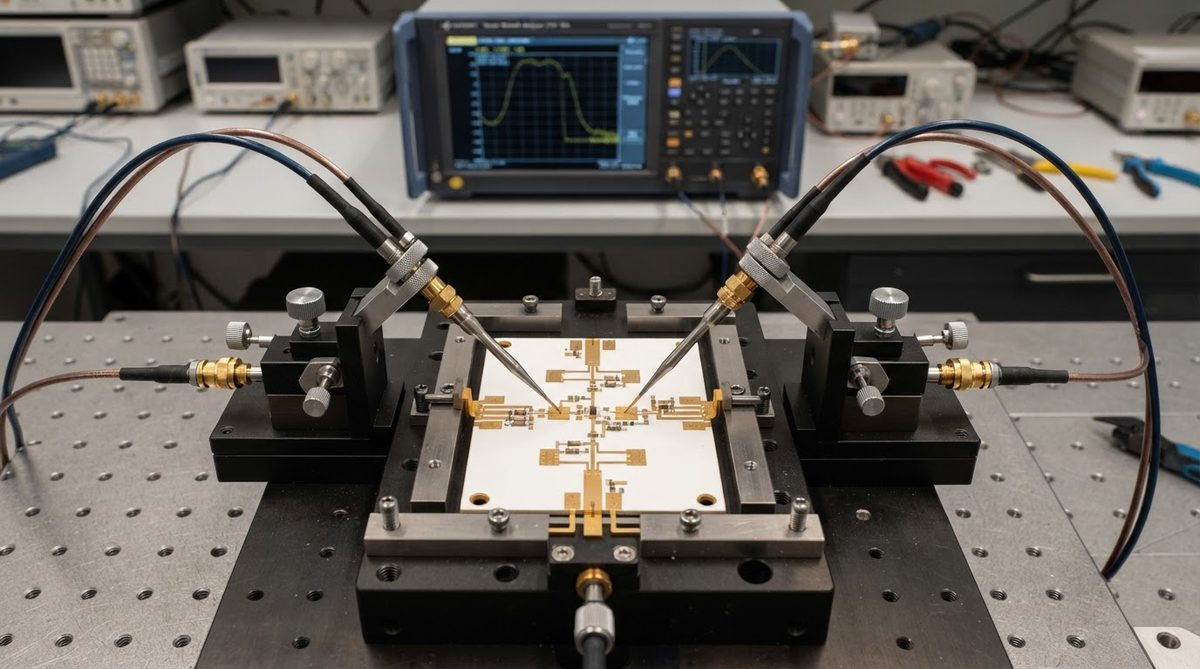
Controlled impedance depends on four variables: trace width (W), substrate height (H), conductor thickness (t), and the substrate’s relative permittivity (εr). On organic laminates, εr shifts with moisture absorption, resin-content variation, and temperature. Ceramic eliminates all three sources of drift.
Alumina 96 % has a dielectric loss tangent below 0.001 at 10 GHz, which keeps signal integrity high while also meaning the real part of εr stays predictable. AlN (εr ≈ 8.5–9.0) is similar in permittivity but offers much higher thermal conductivity (170–200 W/mK), useful when impedance-controlled power amplifier traces must also dissipate heat. For detailed thermal data, see the ceramic thermal conductivity reference table.
The trade-off: a higher εr than FR-4 means the 50 Ω microstrip trace on 0.635 mm alumina is roughly 0.58 mm wide—about half the width it would be on 0.635 mm FR-4. That demands metallization processes with ±0.015 mm or better line-width control, which is readily achieved with thin-film or DPC but tighter than standard thick-film screen printing (±0.05 mm typical).
Microstrip Impedance on Ceramic: Worked Example
The most common controlled-impedance geometry on a single-layer ceramic PCB is microstrip: a signal trace on top, a continuous ground plane on the bottom, separated by the ceramic dielectric.
Using the Hammerstad–Jensen closed-form approximation (per IPC-2141A, Section 4.2.1):
Given: εr = 9.6 (96 % Al₂O₃), H = 0.635 mm, t = 0.010 mm (thin-film gold), target Z₀ = 50 Ω.
Step 1 — Effective permittivity estimate:
εeff ≈ (εr + 1)/2 + (εr − 1)/2 × (1 + 12 H/W)^−0.5. For a first guess of W/H ≈ 0.9 (W ≈ 0.57 mm), εeff ≈ 6.75.
Step 2 — Impedance check:
Z₀ = (120π / √εeff) × 1 / (W/H + 1.393 + 0.667 ln(W/H + 1.444)) ≈ 50.3 Ω. Close enough for a starting geometry; a 2D field solver refines it.
Step 3 — Sensitivity analysis:
If H varies by ±0.025 mm (a realistic ceramic tolerance), Z₀ shifts by roughly ±2 Ω (±4 %). If W varies by ±0.015 mm (thin-film tolerance), Z₀ shifts by ±1.3 Ω (±2.6 %). Combined RSS: ±4.8 %, well within a ±5 % impedance spec.
Enter your substrate material, thickness, and target impedance below to calculate the required trace width and see how manufacturing tolerances affect the result.
[pcb_calc type=”microstrip-impedance”]
Material Comparison for Impedance-Controlled Lines
| Parameter | Al₂O₃ 96 % | Al₂O₃ 99.6 % | AlN | LTCC (Ferro A6M) | FR-4 (ref.) |
|---|---|---|---|---|---|
| εr (1 MHz) | 9.4–9.8 | 9.7–10.1 | 8.5–9.0 | 5.7–5.9 | 4.3–4.5 |
| εr tolerance (lot-to-lot) | ±1.5 % | ±1 % | ±2 % | ±2 % | ±5–10 % |
| tan δ (10 GHz) | 0.0002–0.001 | 0.0001–0.0003 | 0.001–0.003 | 0.002–0.004 | 0.018–0.025 |
| Thickness tolerance (mm) | ±0.025 | ±0.013 | ±0.025 | ±0.015 (per layer) | ±0.05–0.08 |
| 50 Ω microstrip W on 0.635 mm (mm) | ≈ 0.58 | ≈ 0.55 | ≈ 0.62 | ≈ 0.88 | ≈ 1.18 |
| Source | CoorsTek ADS-96R | Kyocera A-493 | Maruwa AN-230 | Ferro A6M datasheet | Isola 370HR |
Typical values for commercially available material, for comparison only. Confirm against the datasheet for your specific grade.
LTCC stands out for multilayer ceramic PCB applications because its lower εr widens the trace, relaxing lithography requirements, while still allowing buried stripline and coplanar waveguide structures within the cofired stack.
Stripline and Coplanar Waveguide Options
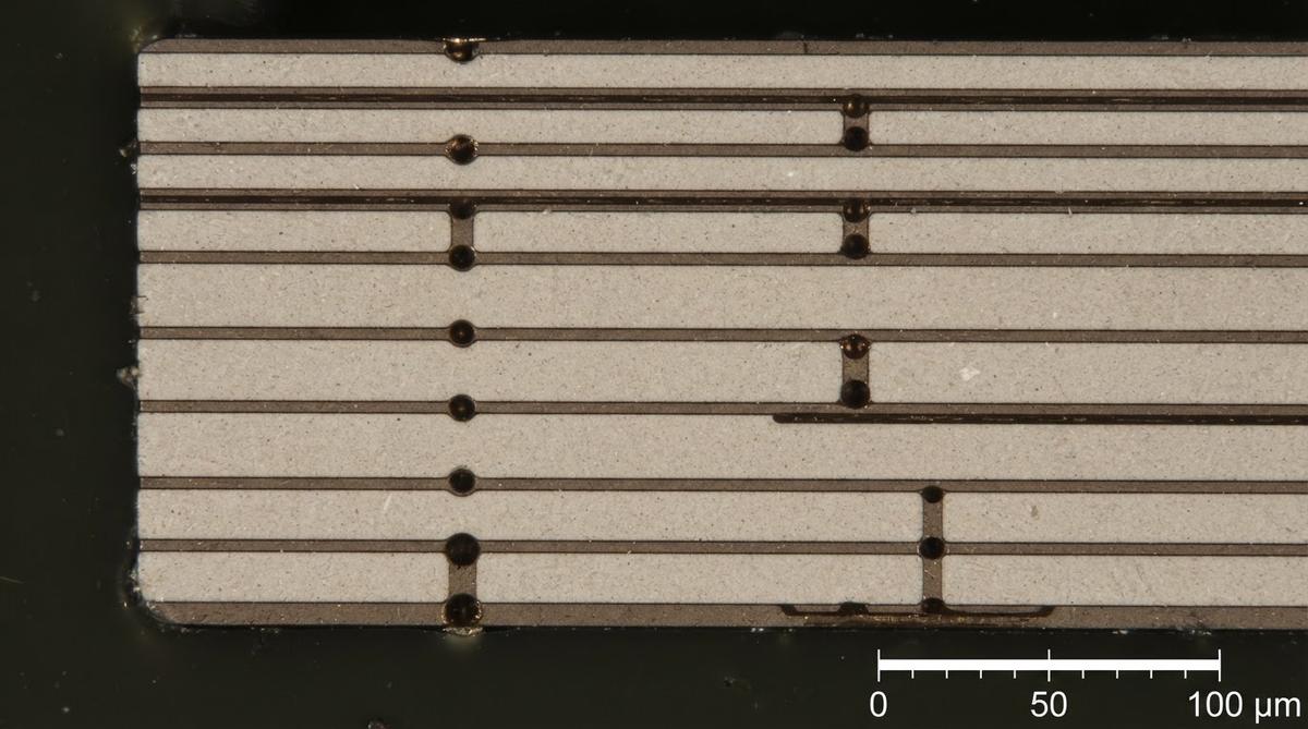
Single-layer ceramic boards are limited to microstrip or coplanar waveguide (CPW). When you need stripline—a signal trace sandwiched between two ground planes—you need at least three conductor layers. On ceramic, this is practical with LTCC (cofired multilayer) or with bonded alumina laminates using glass-frit or epoxy interlayers.
Coplanar waveguide with ground (CPWG) is popular on single-layer ceramic because it provides a ground reference on the same surface as the signal, reducing via inductance and simplifying probe testing. The gap between signal and coplanar ground is the primary impedance-setting dimension. On 96 % alumina, a 50 Ω CPWG with a 0.30 mm signal trace typically needs gaps of about 0.15 mm—achievable with thin-film or metallized ceramic substrate processes using DPC.
Design Rules for Hitting Your Impedance Target
1. Specify substrate thickness and εr on the drawing
Call out the ceramic grade (e.g., “96 % Al₂O₃ per CoorsTek ADS-96R or equivalent”) and the nominal thickness with tolerance. Do not leave it to the fabricator to choose.
2. Use a 2D field solver, not formulas, for final geometry
Closed-form equations are good for initial sizing. Final trace widths should come from a 2D electromagnetic solver (Sonnet, HFSS, or the free ATLC tool) that accounts for conductor thickness, edge profile, and the ground-plane gap in CPW.
3. Match metallization process to line-width tolerance
Thin-film sputtering and DPC hold ±0.010–0.015 mm. Thick-film screen printing holds ±0.03–0.05 mm. If your impedance budget demands ±3 % or tighter, thin-film or DPC is the right call. For broader tolerances (±7–10 %), thick film is cheaper and sufficient.
4. Add TDR coupons
Include time-domain reflectometry test coupons on every panel. This is standard practice on organic controlled-impedance boards and equally important on ceramic. Specify the coupon geometry and acceptance window in your fabrication notes. Impedance verification fits naturally into a broader ceramic PCB quality control flow.
5. Account for surface finish thickness
A 3–5 µm ENIG or gold metallization layer adds to conductor thickness and slightly lowers impedance. Include it in the solver model.
When NOT to Use Ceramic for Impedance Control
Ceramic is overkill—and too expensive—if your impedance tolerance is ±10 % or looser, your frequency is below 1 GHz, and your operating temperature stays under 130 °C. Standard controlled-impedance FR-4 or Rogers RO4003C (εr ≈ 3.55, tan δ ≈ 0.0027 at 10 GHz) will meet the spec at a fraction of the cost.
Ceramic also becomes difficult when you need more than four or five routed layers with impedance control on each. LTCC can do it, but the cost and lead time climb steeply. High-layer-count organic RF laminates (Megtron 6, RO4000 series) may be a better fit for complex digital-RF hybrids.
If your board is larger than about 150 mm × 150 mm, ceramic panel-size limits and warpage risk make organic substrates more practical. Consult the warpage and flatness guide for size-dependent constraints.
Frequently Asked Questions
Can I get 50 Ω controlled impedance on a standard alumina substrate?
Yes. A 50 Ω microstrip on 0.635 mm, 96 % alumina requires a trace width of roughly 0.55–0.60 mm, which thin-film and DPC processes achieve routinely. Thinner substrates (0.25–0.38 mm) narrow the trace further and may require DPC or photolithographic patterning.
How does temperature affect impedance on ceramic?
Very little. The εr of 96 % alumina changes less than 0.5 % from −55 °C to +200 °C (per CoorsTek ADS-96R datasheet), shifting a 50 Ω line by roughly ±0.1 Ω. This is an order of magnitude more stable than FR-4, where moisture and Tg transitions can shift εr by several percent.
What impedance tolerance should I specify on a ceramic PCB?
±5 % is a realistic and commonly met tolerance for thin-film or DPC metallization on alumina with standard substrate thickness control. Specifying ±3 % is possible but requires 99.6 % alumina or tighter incoming substrate screening, which adds cost.
Is thick-film metallization good enough for controlled impedance?
It depends on the tolerance. Thick-film screen printing holds line widths to about ±0.03–0.05 mm, which yields impedance control in the ±7–10 % range on typical substrates. For ±5 % or tighter, thin-film or DPC is preferred.
Do I need a ground plane on the back side for microstrip?
Yes. A continuous, unbroken ground metallization on the opposite face of the substrate is essential for microstrip impedance control. Any gaps, slots, or vias in the ground plane alter the local impedance and must be modeled.
Can LTCC achieve buried stripline with controlled impedance?
Yes. LTCC cofired multilayer processes embed signal traces between ground-plane layers with per-layer thickness control of ±0.015 mm. This enables stripline and broadside-coupled differential pairs inside the ceramic stack, commonly used in radar T/R modules and mmWave front-end packages.
Next Step
If you have a target impedance and a preferred ceramic material, send your stackup and Gerber files for a design-for-manufacturability review. Our engineers will run a 2D field-solver check and confirm achievable trace geometry and tolerance before quoting. Browse the ceramic PCB FAQ for additional design and process questions, or request a quote directly.