OSP (Organic Solderability Preservative) is a thin organic coating—typically 0.2–0.5 µm of benzimidazole or substituted benzimidazole—applied over exposed copper to prevent oxidation before soldering. On ceramic PCBs with DPC or thick-film copper metallisation, OSP is technically feasible and is the lowest-cost finish available. However, its limited shelf life (typically 6 months), poor wire-bondability, and narrow reflow window make it a niche choice for ceramic substrates, where boards often sit in inventory longer and face harsher thermal profiles than standard FR-4 assemblies.
Key Takeaways
- OSP adds 0.2–0.5 µm of organic film over copper and costs roughly 30–50% less per panel than ENIG.
- Shelf life is 6 months under controlled storage (< 30 °C, < 60% RH, sealed bag with desiccant), versus 12+ months for ENIG.
- OSP supports a maximum of 2–3 lead-free reflow cycles before solderability degrades significantly, per IPC J-STD-003C testing.
- The finish is transparent and cannot be visually inspected for coverage without wetting-balance or solderability testing.
- For ceramic boards destined for power modules, RF assemblies, or wire bonding, ENIG, immersion silver, or electroplated gold are almost always better choices.
How OSP Is Applied to Ceramic PCBs
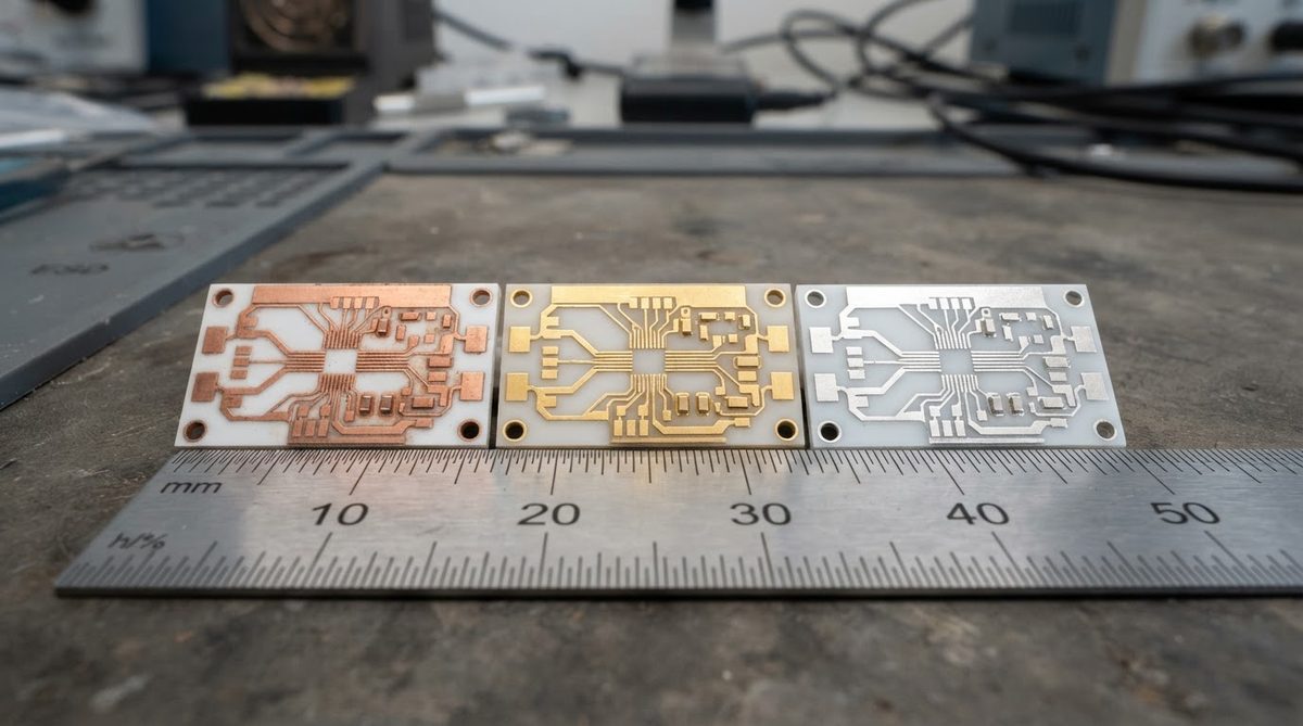
The OSP process on a ceramic substrate follows the same chemistry as on FR-4, but the substrate itself introduces differences. Ceramic boards with DPC (Direct Plated Copper) or thick-film copper traces are cleaned, micro-etched to roughen the copper surface, and then immersed in an acidic OSP bath. The organic molecules selectively adsorb onto copper, forming a uniform film that blocks oxygen and moisture.
Because the ceramic substrate (Al₂O₃, AlN) is chemically inert, the OSP bath does not attack or absorb into the base material the way it can with organic laminates. This is an advantage: there is no risk of subsurface absorption weakening adhesion. The disadvantage is that any exposed ceramic area adjacent to copper pads offers no mechanical key for the OSP film, so the coating terminates sharply at the copper edge. Proper pad design and clean etch-back matter more on ceramic than on FR-4.
OSP Performance Limits on Ceramic Substrates
Most ceramic PCB applications involve high temperatures, long storage, or multiple thermal cycles. OSP struggles with all three.
Shelf Life and Storage
OSP-coated boards must be stored in sealed, nitrogen-flushed bags with desiccant at below 30 °C and 60% RH. Even under ideal conditions, solderability begins to degrade after 6 months. Ceramic boards used in power electronics or aerospace often have procurement-to-assembly lead times of 3–9 months, which can consume most or all of the OSP shelf life before the board reaches the reflow oven.
Reflow Cycle Tolerance
Each lead-free reflow cycle (peak 245–260 °C for SAC305) partially decomposes the organic film. After 2 reflows, wetting force measured per IPC J-STD-003C typically drops below acceptable thresholds. ENIG, by contrast, tolerates 4–6 reflows with no measurable solderability loss. If your assembly involves double-sided reflow or rework, OSP is a risky choice.
Wire Bonding
OSP is incompatible with gold or aluminium wire bonding. The organic layer must be removed before bonding, and the exposed copper oxidises within minutes in ambient air. For any ceramic PCB that requires wire bonding—common in semiconductor packaging on AlN substrates—use ENIG, ENEPIG, or electroplated gold instead.
OSP vs ENIG vs Immersion Silver on Ceramic PCBs
The table below compares the three most common finishes applied to copper-metallised ceramic substrates. Data reflects typical commercial-grade chemistry; confirm values with your finish supplier’s technical data sheet.
| Parameter | OSP | ENIG | Immersion Silver | Condition / Source |
|---|---|---|---|---|
| Thickness | 0.2–0.5 µm | 3–6 µm Ni / 0.05–0.1 µm Au | 0.15–0.40 µm Ag | Per IPC-4552 (ENIG), IPC-4553 (ImAg) |
| Shelf life (sealed storage) | 6 months | 12+ months | 6–12 months | < 30 °C, < 60% RH |
| Max reflow cycles (SAC305) | 2–3 | 4–6 | 3–4 | Peak 260 °C, per J-STD-003C |
| Wire bondable | No | Yes (Au wire) | No | — |
| Contact resistance | Moderate (bare Cu after flux) | Low | Low | — |
| Relative cost per panel | 1× (baseline) | 2–3× | 1.3–1.8× | Typical pricing, 96% Al₂O₃ substrate |
| Coplanarity for fine pitch | Excellent | Good | Excellent | — |
Typical values for commercially available materials, for comparison only. Confirm against the datasheet for your specific grade.
Use the tool below to compare estimated finish costs across different panel sizes and quantities. Enter your substrate dimensions and annual volume to see a side-by-side breakdown.
[pcb_calc type=”finish-cost”]
When OSP Makes Sense on a Ceramic Board
OSP is a reasonable choice when all of the following are true:
- Assembly happens within 4 weeks of board delivery (short supply chain).
- Only one reflow pass is required—single-sided SMT, no rework planned.
- No wire bonding or press-fit connectors are used.
- The operating environment does not expose bare pads to humidity (conformal coat or encapsulation is applied post-assembly).
- Cost pressure is significant enough that the 2–3× ENIG premium matters at your volume.
A common example: high-volume LED alumina ceramic substrates where the die is adhesive-bonded (not wire-bonded) and reflowed once. In this scenario, OSP delivers adequate solderability at the lowest finish cost.
When NOT to Use OSP on Ceramic PCBs
For most ceramic PCB projects, OSP is not the right default. Avoid it when:
- Long storage is expected. Power module substrates and aerospace boards often sit in inventory for months. ENIG or electroplated gold handle this far better.
- Multiple reflows or rework. Double-sided assembly or expected rework cycles demand a finish that survives 4+ reflows.
- Wire bonding is required. Any die-attach process using Au or Al wire needs a metallic finish—ENIG, ENEPIG, or thick gold.
- High-frequency RF circuits. OSP residue after soldering can introduce dielectric variability at the pad interface. Immersion silver or ENIG gives more predictable RF performance.
- Harsh environments without conformal coat. Exposed OSP-finished pads in humid or corrosive atmospheres degrade rapidly.
In these cases, consult the full comparison of ceramic PCB surface finishes to select the right alternative.
Worked Example: OSP vs ENIG Cost on a 50 × 50 mm Alumina Panel
Assume a 96% Al₂O₃ DPC substrate, 50 × 50 mm, 0.635 mm thick, single-sided, 200 pcs.
- OSP finish cost contribution: approximately $0.15–$0.25 per board (chemistry + labour).
- ENIG finish cost contribution: approximately $0.40–$0.70 per board.
- Savings with OSP: ~$0.25–$0.45 per board, or $50–$90 across a 200-piece lot.
That saving is meaningful at consumer LED volumes. For a 50-piece power module prototype where a single assembly failure costs $200+ in rework, the $10–$20 total ENIG premium is trivial insurance. Choose the finish that matches your risk profile, not the one that looks cheapest on the BOM.
FAQ
Can OSP be applied over thick-film copper on ceramic?
Yes. The OSP bath adsorbs onto any exposed copper surface regardless of how the copper was deposited. Thick-film, DPC, and plated copper all accept OSP chemistry. The ceramic substrate itself is inert and unaffected by the bath.
Does OSP outgas at high temperatures?
OSP begins to decompose above 200 °C and is fully removed during a standard lead-free reflow at 245–260 °C peak. For applications with sustained operating temperatures above 150 °C, the finish is gone post-reflow and provides no ongoing protection. Post-assembly conformal coating or hermetic sealing is needed to protect exposed copper.
Can I rework an OSP-finished ceramic board?
Rework is possible but risky. The OSP film is consumed during the first reflow, so any rework exposes bare copper that oxidises rapidly. Applying flux before rework helps, but solderability is noticeably worse than reworking an ENIG-finished board. If rework is likely, specify ENIG or immersion silver from the start.
Is OSP RoHS and REACH compliant?
Yes. Modern OSP chemistries (benzimidazole-based) contain no restricted substances under RoHS 3 (EU 2015/863) or REACH SVHC lists. OSP is one of the most environmentally benign finishes available, with no heavy metals in the coating or the waste stream.
How do I verify OSP coverage on a ceramic board?
Visual inspection is unreliable because the film is transparent and only 0.2–0.5 µm thick. The standard method is a wetting-balance test per IPC J-STD-003C or a solderability test per IPC-TM-650 2.4.14. Some manufacturers use UV fluorescence to screen for gross defects, but quantitative thickness measurement requires X-ray fluorescence (XRF) or ellipsometry.
Next Step
If you are evaluating surface finishes for a ceramic PCB project, start by defining your assembly process, storage timeline, and operating environment. Review the ceramic PCB manufacturing process to understand how finish selection interacts with metallisation choices. When you are ready to compare options on your specific board, request a quote and our engineers will recommend the finish that fits your application.