Gold metallized ceramic substrates are ceramic boards—typically alumina (Al₂O₃) or aluminum nitride (AlN)—with a patterned gold conductor layer deposited by thick-film screen printing or thin-film sputtering. A gold metallized ceramic board is chosen where corrosion resistance, wire-bond reliability, or long-term contact stability matters more than conductor cost. The gold layer thickness ranges from 0.1–0.5 µm for thin-film processes to 5–15 µm for thick-film prints, and the choice between them drives most of the performance and cost differences engineers care about.
Key Takeaways
- Thick-film gold on 96% alumina is the most common gold metallized ceramic configuration, with fired conductor resistivity of 3–5 mΩ/sq at 10 µm thickness (per Heraeus C8729 datasheet).
- Thin-film gold (Ti/Pt/Au or Ti/Ni/Au stacks) achieves line/space below 25 µm, making it suitable for RF and MEMS packaging.
- Gold wire bonding to a gold-metallized pad is the most reliable interconnect in hermetic packages, with shear strengths exceeding 60 MPa per MIL-STD-883 Method 2019.
- Gold metallization costs 3–8× more than silver and 5–12× more than copper per unit area, depending on layer thickness and deposition method.
- For high-current or broad-area conductors where corrosion is manageable, silver metallized ceramic or copper-based processes offer far better cost-per-amp performance.
Thick-Film vs Thin-Film Gold Metallized Ceramic Processes
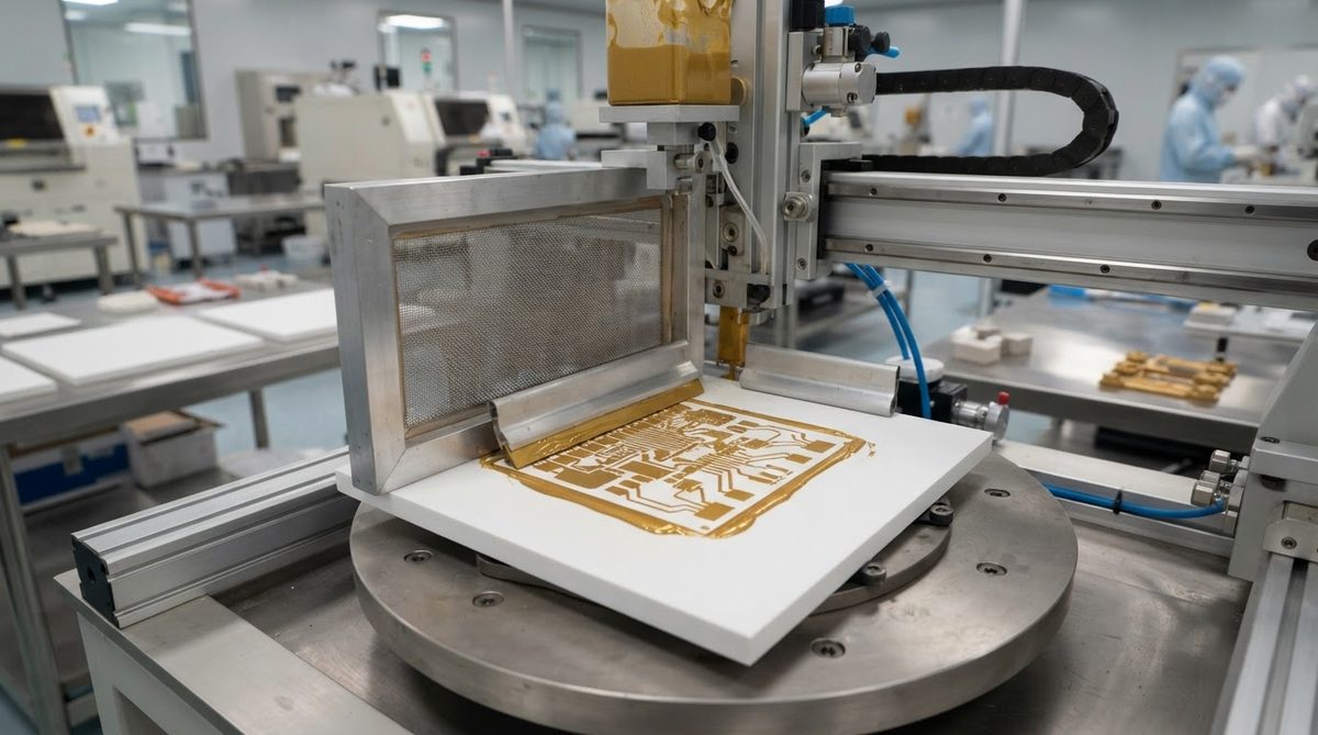
Thick-film gold is screen-printed as a paste (gold powder in a glass frit and organic binder) onto a fired ceramic substrate, then sintered at 850–950 °C. The result is a dense but slightly porous conductor, 5–15 µm thick, with sheet resistance of 3–5 mΩ/sq at 10 µm. Minimum line/space is typically 100–125 µm. Thick-film gold bonds well with both gold and aluminum wire and is the standard for hybrid microelectronics and hermetic packages.
Thin-film gold is deposited by sputtering or e-beam evaporation, usually as part of a multi-layer stack: an adhesion layer (Ti or Cr, 20–50 nm), a barrier/diffusion layer (Pt, Ni, or W, 50–200 nm), and the gold conductor (0.1–0.5 µm, plated up to 1–3 µm where needed). Sheet resistance is lower per unit thickness because the film is fully dense—roughly 2.4 mΩ/sq at 1 µm. Minimum line/space reaches 10–25 µm with photolithographic patterning. Thin-film gold metallized ceramic substrates are preferred for RF circuits, MEMS sensor packaging, and any layout requiring fine geometry.
| Parameter | Thick-Film Au | Thin-Film Au | Unit | Condition / Source |
|---|---|---|---|---|
| Typical thickness | 5–15 | 0.1–3 (plated up) | µm | Heraeus, DuPont datasheets |
| Sheet resistance | 3–5 | 2–3 | mΩ/sq | At 10 µm / at 1 µm |
| Min line/space | 100–125 | 10–25 | µm | Screen print vs photolith |
| Adhesion to 96% Al₂O₃ | 15–30 | 20–40 | MPa | Pull test, ASTM F1842 |
| Firing / process temp | 850–950 | ≤300 (sputter + cure) | °C | — |
| Solder wettability | Good (with Ni barrier) | Good (with Ni/Pt barrier) | — | AuSn, SnAgCu solders |
| Wire bond compatibility | Au ball, Al wedge | Au ball, Al wedge | — | MIL-STD-883 Method 2011 |
Typical values for commercially available material, for comparison only. Confirm against the datasheet for your specific grade.
Why Choose Gold Metallized Ceramic Over Silver or Copper?
Gold does not oxidize or tarnish in ambient conditions. Silver tarnishes in sulfur-containing atmospheres, forming resistive Ag₂S films that degrade solder joints and wire bonds over months. Copper oxidizes rapidly above 200 °C and requires protective plating. In hermetically sealed packages, military hybrids, implantable medical devices, and space-qualified electronics, gold’s chemical inertness eliminates a failure mode entirely.
Gold also forms the most reliable thermosonic ball bond in the industry. Au-Au ball bonds on 96% alumina thin-film substrates routinely pass 1,000-hour HTOL (high-temperature operating life) at 175 °C without bond degradation, per JEDEC JESD22-A108. This is why gold metallization dominates in Class 3 (high-reliability) assemblies per IPC J-STD-001.
The trade-off is cost. Gold spot prices fluctuate, but a thick-film gold conductor layer adds roughly $0.15–$0.50/cm² to the substrate cost at 8–12 µm thickness, versus $0.02–$0.06/cm² for silver. For designs where corrosion can be managed with conformal coating or nitrogen atmosphere, silver or copper metallization is far more economical.
Common Substrate Materials for Gold Metallized Ceramic Boards
Gold metallization is compatible with most oxide and nitride ceramics. The two most common pairings are 96% alumina and 99.6% alumina. AlN substrates also accept gold, typically via thin-film sputtering with a TiW or Ti adhesion layer, for high-power applications that need both thermal conductivity (170–200 W/mK) and reliable wire bonding.
Substrate choice affects the metallization process. 99.6% alumina thick-film substrates have a finer grain structure and smoother surface (Ra < 0.3 µm lapped), which improves thin-film adhesion and line definition. Standard 96% alumina (Ra 0.4–0.8 µm as-fired) works well for thick-film gold but may need lapping for thin-film processes. Substrate dimensions are available in standard ceramic substrate sizes from 2″×2″ to 4.5″×4.5″ panels.
Worked Example: Gold Metallization Cost per Substrate
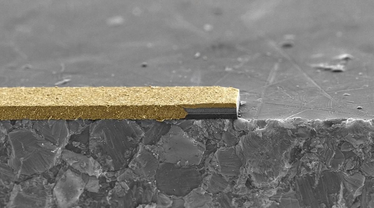
Assume a 25.4 mm × 25.4 mm (1″ × 1″) gold metallized ceramic substrate with 40% gold coverage, thick-film printed at 10 µm fired thickness.
- Substrate area: 6.45 cm². Gold coverage area: 6.45 × 0.40 = 2.58 cm².
- Gold volume: 2.58 cm² × 0.001 cm = 0.00258 cm³.
- Gold mass: 0.00258 cm³ × 19.3 g/cm³ = 0.0498 g ≈ 0.05 g.
- At a gold price of $75/g (approximate mid-2025 spot), raw gold cost per substrate ≈ $3.75.
- Paste cost includes glass frit, vehicle, and supplier margin—typically 1.5–2× raw metal cost for thick-film paste. Estimate $5.60–$7.50 in paste per substrate.
- Add printing, drying, and firing labor/overhead: $2–$4 per substrate in production volumes (500+ pcs).
- Total gold metallization cost contribution: roughly $7.60–$11.50 per 1″ × 1″ substrate at 40% coverage.
The same geometry in silver thick-film paste would cost $0.80–$1.50 in metal and paste. This 5–8× cost multiple is why gold metallized ceramic is reserved for applications where no alternative meets the reliability requirement.
When NOT to Use Gold-Metallized Ceramic
Gold is the wrong choice in several common scenarios:
- High-current power circuits. Gold’s thin layers (5–15 µm) carry far less current than 100–300 µm copper on DBC or AMB substrates. If your design dissipates more than a few watts per conductor, copper metallization is the practical option.
- Cost-sensitive consumer products. For LED boards, sensor arrays, or IoT modules where the operating environment is benign, silver or copper metallization delivers equivalent electrical performance at a fraction of the cost.
- Large-area ground planes. Gold’s cost scales linearly with coverage area. A 50 mm × 50 mm ground plane in gold is prohibitively expensive. Use copper or silver with a protective finish instead.
- Designs requiring thick conductors for thermal spreading. Gold is not available in the 100+ µm thicknesses that DBC or copper-metallized ceramic substrates provide.
Frequently Asked Questions
Can you solder directly to gold-metallized ceramic?
Yes. Gold-metallized pads are solderable with AuSn (80/20) eutectic solder, SnAgCu (SAC305), and other common alloys. A nickel barrier layer (2–5 µm) underneath the gold prevents gold embrittlement of the solder joint—sometimes called “gold scavenging”—when the gold layer exceeds 0.5 µm. Most thick-film gold systems include this barrier by design.
Does gold metallization work on aluminum nitride?
Yes. Gold is deposited on AlN substrates via thin-film sputtering (Ti/Pt/Au or TiW/Au stacks) or thick-film printing with AlN-compatible pastes. The adhesion layer is critical because AlN’s surface chemistry differs from alumina. Properly processed Au on AlN achieves adhesion above 20 MPa per ASTM F1842. See AlN thin-film substrates for available configurations.
What is the shelf life of gold-metallized ceramic substrates?
Gold does not tarnish or oxidize under normal storage conditions. Gold metallized ceramic substrates stored in dry, clean packaging remain solderable and wire-bondable for years—far longer than silver or copper, which require controlled atmosphere or vacuum packaging to prevent surface degradation. A practical shelf life of 5+ years is common for gold-metallized parts stored per MIL-STD-1686 ESD precautions.
Is gold metallization compatible with HTCC and LTCC processes?
Gold is compatible with LTCC co-firing (peak temperatures 850–900 °C), where it serves as an internal and external conductor. Gold is not used in HTCC (peak temperatures 1,500–1,600 °C) because gold melts at 1,064 °C. HTCC uses tungsten or molybdenum internal conductors, with gold applied as a post-fire plating or thick-film overprint.
How does gold compare to platinum or palladium metallization?
Platinum and palladium are also noble metals used on ceramic substrates, but their sheet resistance is 3–5× higher than gold at equivalent thickness. Pt and Pd are chosen for resistor elements, sensor electrodes, or environments above 500 °C where gold softens. For standard interconnect and wire-bond pads, gold offers the best combination of conductivity and bondability.
Next Step
If your design calls for gold metallized ceramic in alumina or AlN, start by defining the conductor thickness, line/space, and substrate material grade. For a budgetary quote on gold metallized ceramic substrates, submit your artwork and specifications through the AluminaPCB quote page.