Ceramic PCBs offer thermal conductivity 10–80× higher than FR-4, a coefficient of thermal expansion (CTE) close to silicon and GaN, and stable dielectric properties into the GHz range—but they cost 5–20× more per unit area, fracture under mechanical shock, and ship in smaller panel sizes with longer lead times. Understanding ceramic PCB advantages disadvantages in concrete terms—with real numbers—lets you decide whether the performance gains justify the cost and handling constraints for your specific board.
Key Takeaways
- 96% alumina (Al₂O₃) delivers 24–28 W/m·K; aluminum nitride (AlN) reaches 170–200 W/m·K, versus 0.25–0.35 W/m·K for FR-4 (per CoorsTek and Kyocera datasheets, measured at 20 °C).
- Ceramic CTE of 6.5–7.4 ppm/°C (Al₂O₃) or 4.4–4.7 ppm/°C (AlN) closely matches silicon (2.6 ppm/°C) and GaN (3.2 ppm/°C), reducing solder-joint fatigue in power and RF die-attach.
- Ceramic substrates are brittle: flexural strength of 300–380 MPa for 96% Al₂O₃ (ASTM C1161) versus effectively infinite ductility in FR-4.
- Unit cost for a 25 × 25 mm ceramic board is typically 5–20× that of an equivalent FR-4 board, depending on material grade and metallization process.
- Maximum standard panel size is roughly 190 × 140 mm for most ceramic processes, compared with 457 × 610 mm for standard FR-4.
Ceramic PCB Advantages Disadvantages at a Glance
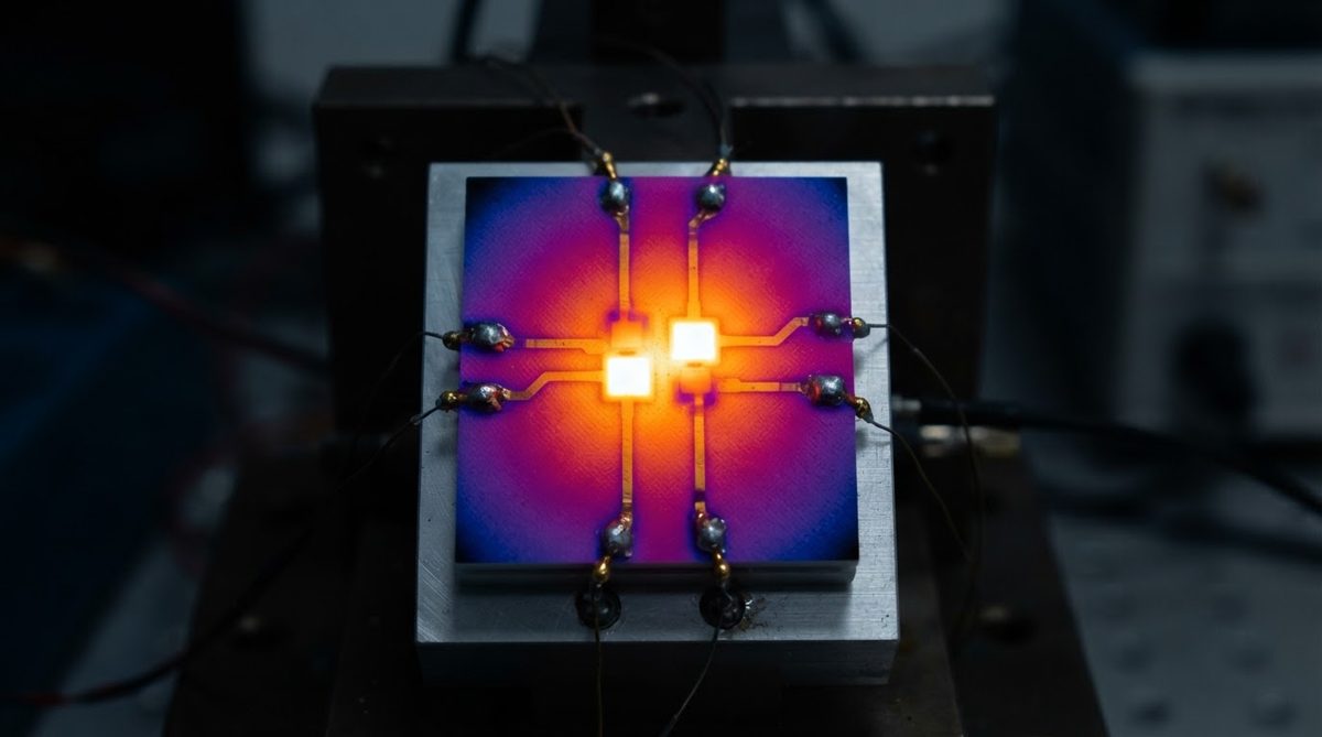
The table below captures the core ceramic PCB advantages disadvantages in a single view. Each row is a measurable parameter, not a subjective rating.
| Parameter | 96% Al₂O₃ Ceramic | AlN Ceramic | FR-4 | Aluminum MCPCB | Unit | Condition / Source |
|---|---|---|---|---|---|---|
| Thermal conductivity | 24–28 | 170–200 | 0.25–0.35 | 1.0–3.0 (dielectric layer) | W/m·K | 20 °C; CoorsTek, Kyocera datasheets |
| CTE (in-plane) | 6.5–7.4 | 4.4–4.7 | 12–16 | 22–24 (Al base) | ppm/°C | 25–300 °C; manufacturer data |
| Dielectric constant (εr) | 9.4–9.8 | 8.5–9.0 | 4.2–4.8 | 4.0–5.0 (dielectric) | — | 1 MHz; Kyocera A-476, IPC-TM-650 |
| Loss tangent (tan δ) | 0.0001–0.0004 | 0.0003–0.001 | 0.018–0.025 | 0.020–0.025 | — | 1 GHz |
| Max continuous temp | 800–1 000 | 800–1 000 | 130 (Tg-dependent) | 130–150 | °C | Substrate only, no metallization limit |
| Flexural strength | 300–380 | 300–350 | 415–480 | N/A (metal) | MPa | ASTM C1161, 4-pt bend |
| Moisture absorption | < 0.01 | < 0.01 | 0.10–0.15 | 0.05–0.10 | % | 24 h, 25 °C; IPC-TM-650 2.6.2 |
| Relative substrate cost | 1× (baseline) | 5–8× | 0.05–0.1× | 0.3–0.5× | — | Per cm², volume pricing |
Typical values for commercially available material, for comparison only. Confirm against the datasheet for your specific grade.
Advantages of Ceramic PCBs
High Thermal Conductivity
The primary reason engineers specify ceramic is heat removal. A 1 mm-thick, 10 × 10 mm AlN substrate dissipating 20 W produces a through-thickness ΔT of roughly 1.0 °C (using k = 185 W/m·K). The same geometry in FR-4 (k ≈ 0.3 W/m·K) yields ΔT ≈ 667 °C—an impossible operating condition. Even 96% alumina at 25 W/m·K keeps ΔT under 8 °C. This is why ceramic substrates are chosen for power electronics and high-brightness LED modules.
For direct-bonded-copper (DBC) and active-metal-brazed (AMB) substrates, thick copper layers (0.3 mm) on ceramic provide both lateral heat spreading and electrical isolation, a combination metal-core PCBs struggle to match at the same voltage rating.
CTE Match to Semiconductor Die
Silicon has a CTE of about 2.6 ppm/°C. FR-4’s in-plane CTE is 12–16 ppm/°C. Under thermal cycling from −40 °C to +150 °C, the CTE mismatch between die and substrate creates shear stress in the solder joint. Ceramic substrates cut that mismatch by half to two-thirds. AlN at 4.5 ppm/°C is particularly well suited for bare-die GaN and SiC power devices, where junction temperatures exceed 175 °C and solder fatigue is the dominant failure mode.
Dielectric Strength and High-Frequency Performance
96% alumina has a dielectric constant (εr) of 9.4–9.8 at 1 MHz (per Kyocera datasheet A-476) and a loss tangent of 0.0001–0.0004 at 1 GHz. The loss tangent is roughly 50× lower than standard FR-4 (tan δ ≈ 0.020). For mmWave filters, couplers, and antenna feed networks above 10 GHz, this translates directly into lower insertion loss and tighter passband control. Dielectric breakdown strength for 0.635 mm alumina exceeds 10 kV/mm (per IEC 60672-3), enabling high-voltage isolation in a thin package.
Chemical and Environmental Stability
Ceramic substrates absorb essentially zero moisture (water absorption < 0.01% for 96% Al₂O₃). They do not outgas, do not support fungal growth, and remain dimensionally stable from cryogenic temperatures up through several hundred degrees Celsius. This matters in downhole oil-and-gas tools, satellite electronics, and implantable medical devices where decades of hermetic reliability are required. For storage considerations, see ceramic PCB shelf life and storage conditions.
Long Operational Life
Because ceramics do not degrade under UV, do not delaminate, and resist most solvents and acids, ceramic PCBs routinely pass 1,000+ thermal shock cycles (−55 °C to +150 °C, per MIL-STD-883 Method 1011) without measurable change in insulation resistance. FR-4 laminates often show delamination or measling after 200–500 cycles under the same conditions.
Disadvantages of Ceramic PCBs
Higher Cost per Unit Area
Raw 96% alumina substrate costs roughly $0.08–$0.15/cm² in volume. AlN runs $0.50–$1.20/cm². FR-4 laminate is $0.005–$0.02/cm². Metallization adds more: DPC (direct plated copper) and DBC processes are batch operations with expensive tooling and atmosphere-controlled furnaces. A finished 25 × 25 mm DBC-on-alumina board in quantities of 500 might cost $4–$8 each; the same footprint in FR-4 is under $0.50.
Worked example: A 50 × 50 mm AlN DPC board at $1.00/cm² substrate cost alone is $25.00 for the raw ceramic. Add metallization, patterning, surface finish, and testing, and the finished unit reaches $45–$70 at 200-piece volumes. The same board in 1.6 mm FR-4 with 2 oz copper is under $3.00. This cost gap is the single largest disadvantage in any ceramic PCB advantages disadvantages analysis.
Brittleness and Mechanical Fragility
Ceramic is a brittle material. It does not yield; it fractures. Flexural strength for 96% Al₂O₃ is 300–380 MPa (ASTM C1161, 4-point bend), but fracture toughness (K_IC) is only 3.5–4.0 MPa·√m—roughly 1/10 that of structural steel. Point loads, overtightened screws, or drop impacts that FR-4 absorbs elastically will crack a ceramic board. Panel handling during assembly requires fixtures, vacuum pick-and-place, and operator training. For information on mechanical processing, see how to drill holes in alumina and AlN substrates.
Limited Panel Size and Layer Count
Most ceramic processes top out at roughly 190 × 140 mm per substrate. LTCC can build multilayer structures (up to 20+ layers), but HTCC, DBC, and DPC are predominantly single- or double-sided. If your design needs a 10-layer stackup in a 200 × 300 mm format, ceramic is not a practical choice. For details on dimensional options, see available ceramic PCB thicknesses.
Longer Lead Times
Prototype ceramic boards typically require 2–4 weeks, versus 3–5 days for standard FR-4 quick-turn. Production runs may take 4–8 weeks. The sintering cycle alone (for HTCC or LTCC) can be 24–48 hours in a high-temperature kiln. If your schedule demands boards next week, FR-4 or aluminum MCPCB will get there faster.
Fewer Fabricators, Smaller Supply Base
The global number of qualified ceramic PCB fabricators is a fraction of the FR-4 supply base. Second-sourcing is harder. Qualification audits take longer. For high-reliability programs (automotive, aerospace, medical), this supply-chain concentration is a genuine risk that procurement teams must plan around.
Use the tool below to see how temperature derating affects your material choice. Enter your operating temperature range and substrate material to visualize thermal margin across the ceramic PCB advantages disadvantages you are weighing.
When a Ceramic PCB Makes Sense
Ceramic substrates earn their cost premium in applications where at least two of these conditions are true simultaneously:
- Thermal flux exceeds 5 W/cm² and the board cannot use a heatsink large enough to compensate for FR-4’s poor conductivity.
- Operating temperature stays above 150 °C continuously, beyond FR-4’s glass-transition range.
- Frequency is above 5 GHz and insertion loss budget is tight.
- CTE match to a bare semiconductor die is required for solder-joint reliability over thousands of thermal cycles.
- The environment demands zero moisture absorption, chemical inertness, or radiation hardness.
If only one condition applies, a cheaper alternative—high-Tg FR-4, polyimide flex, or metal-core PCB—may satisfy the requirement at a fraction of the cost.
When NOT to Use a Ceramic PCB
Ceramic is the wrong choice when:
- The board is large. Anything beyond roughly 150 × 100 mm becomes impractical or requires panelization with yield risk.
- Layer count exceeds 4–6 and the budget is limited. LTCC can go higher, but cost escalates steeply. A 10-layer FR-4 is vastly cheaper.
- Mechanical shock or vibration is severe. Consumer handhelds, automotive body-mounted sensors, and anything that gets dropped repeatedly will crack ceramic. Use FR-4 or flex-rigid instead.
- Time-to-market is critical. If you need prototypes in five days, FR-4 quick-turn services deliver. Ceramic does not.
- Thermal load is moderate. Below 2 W/cm², a standard 1.6 mm FR-4 board with thermal vias and a copper pour often suffices. Adding ceramic substrate cost here buys nothing.
- Cost target is consumer-grade. At volumes above 10,000 units, ceramic’s per-unit cost rarely fits a consumer BOM. Exceptions exist (LED COB modules), but they are narrow.
Decision Checklist: Is Ceramic Right for Your Board?
Run through these six questions against your design. If you answer “yes” to three or more, ceramic deserves a serious evaluation based on the ceramic PCB advantages disadvantages outlined above. If fewer than two, start with FR-4 or MCPCB and revisit only if testing shows a thermal or reliability gap.
- Is the peak thermal flux at any component above 5 W/cm²?
- Will the board operate continuously above 150 °C?
- Does the design carry signals above 5 GHz where loss tangent matters?
- Are you attaching bare die (flip-chip, wire-bond, or sintered silver) directly to the substrate?
- Must the board survive 1,000+ thermal shock cycles (e.g., automotive AEC-Q100 Grade 1)?
- Is the operating environment corrosive, high-humidity, or high-radiation?
Frequently Asked Questions
Can ceramic PCBs be made with multiple layers?
Yes. LTCC (low-temperature co-fired ceramic) supports multilayer stackups of 20 or more layers with embedded passives and vias. HTCC also allows multilayer construction but at higher sintering temperatures (1,400–1,600 °C), which limits conductor materials to tungsten or molybdenum. DBC and DPC processes are limited to one or two metal layers per substrate.
Is a ceramic PCB heavier than FR-4?
Yes. 96% alumina has a density of 3.7–3.9 g/cm³ versus 1.8–1.9 g/cm³ for FR-4. A 50 × 50 × 0.635 mm alumina substrate weighs roughly 5.9 g; the same volume in FR-4 weighs about 2.9 g. For weight-sensitive aerospace or wearable applications, this difference matters and should be included in the mass budget early.
What surface finishes work on ceramic boards?
Common finishes include ENIG (electroless nickel / immersion gold), ENEPIG, thick gold plating, and bare copper with OSP. The choice depends on the solder alloy and attach method. For wire bonding, gold or silver thick-film pads are typical. For reflow soldering, ENIG or ENEPIG provides reliable wetting and shelf life.
Do ceramic PCBs need conformal coating?
Generally no. The ceramic substrate itself is impervious to moisture and most chemicals. Conformal coating may still be applied to protect solder joints and copper traces from corrosion in harsh environments, but the substrate does not require it for moisture protection the way FR-4 does.
How do you prototype with ceramic if lead times are long?
Order blank substrates in standard sizes and use laser-patterned DPC metallization, which has shorter setup time than screen-printed thick film. Some fabricators offer 10–15 day prototype service for simple single-layer DPC designs. Alternatively, validate your thermal design on an aluminum MCPCB first, then move to ceramic for qualification builds. You can also order a single ceramic PCB for early-stage evaluation.
Are there health hazards with ceramic PCB materials?
Alumina and aluminum nitride are considered non-hazardous in finished form. AlN dust can be irritating if machined without extraction, but the sintered substrate poses no toxicity risk in normal handling. Beryllium oxide (BeO) is a different matter entirely: BeO dust is a confirmed human carcinogen. See the full safety discussion at is beryllia dangerous before considering BeO for any design.
Last reviewed: 2025-07.