A DBC substrate is a ceramic base—typically Al₂O₃ or AlN—with copper foil bonded directly to one or both faces through a high-temperature oxidation process, without adhesives or solder. If you are asking what is DBC substrate in practical terms: the resulting composite carries high current, spreads heat efficiently, and matches the CTE of semiconductor die far better than metal-core PCBs. DBC is the dominant substrate technology inside IGBT modules, high-power LED arrays, and SiC/GaN power converters.
Key Takeaways
- DBC bonds copper to ceramic at roughly 1065–1083 °C using a thin Cu₂O eutectic layer, producing a joint stronger than the ceramic itself.
- Thermal conductivity of the composite depends on the ceramic: 24–28 W/mK for 96% Al₂O₃, 170–200 W/mK for AlN (per CoorsTek and Kyocera datasheets).
- Standard copper thickness on DBC ranges from 0.127 mm (5 mil) to 0.635 mm (25 mil), enabling direct die-attach and wire bonding.
- DBC is not suitable for fine-pitch RF traces or multilayer routing; DPC (direct plated copper) or LTCC serve those roles better.
What Is DBC Substrate and How Does the Bonding Process Work?
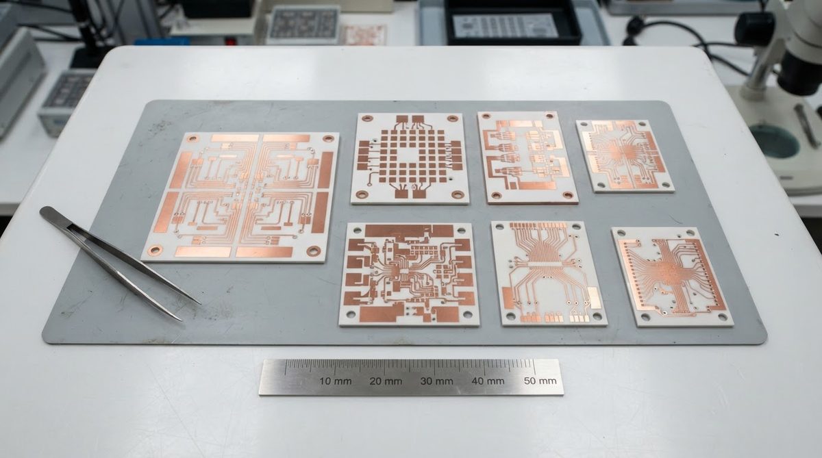
The name says it all: copper bonds directly to ceramic. The mechanism relies on a controlled oxide interlayer. Copper foil is pre-oxidized or placed in a nitrogen-oxygen atmosphere and heated to just below copper’s melting point (1085 °C). At 1065–1083 °C, a Cu–Cu₂O eutectic liquid forms at the interface. This liquid wets the ceramic surface, and on cooling it solidifies into a thin crystalline bond layer roughly 1–3 µm thick.
The bond is chemical, not mechanical. Peel strength typically exceeds 4 N/mm per IEC 60249-2, and in practice the ceramic fractures before the copper delaminates. After bonding, the copper is patterned by standard photolithography and etching—the same workflow used for etching copper on ceramic substrates.
Common Ceramic Materials Used in a DBC Substrate
The ceramic base determines thermal performance, cost, and mechanical reliability. Two materials dominate commercial DBC production; a third serves niche high-performance roles.
| Parameter | Al₂O₃ 96% | AlN | Si₃N₄ | Unit | Condition |
|---|---|---|---|---|---|
| Thermal conductivity | 24–28 | 170–200 | 70–90 | W/mK | 20 °C, per Kyocera / Maruwa datasheets |
| CTE | 6.5–7.2 | 4.4–4.7 | 2.5–3.2 | ppm/°C | 20–300 °C |
| Flexural strength | 300–380 | 300–400 | 600–900 | MPa | ASTM C1161, 3-pt bend |
| Dielectric strength | ≥ 10 | ≥ 15 | ≥ 12 | kV/mm | AC, per manufacturer data |
| Relative cost | 1× | 3–5× | 5–8× | — | Normalized to Al₂O₃ 96% |
Typical values for commercially available material, for comparison only. Confirm against the datasheet for your specific grade.
96% alumina covers the majority of DBC substrate applications below 150 W. For higher power densities or SiC die (which run hotter), aluminum nitride (AlN) becomes necessary because its thermal conductivity is 6–8× higher than alumina. Si₃N₄ is chosen when thermal cycling reliability matters more than raw conductivity—its high fracture toughness resists crack propagation under repeated –40 to +150 °C swings in automotive traction inverters.
Worked Example: Thermal Resistance of a DBC Substrate Stack
Suppose you have a 0.32 mm AlN DBC substrate, 10 × 10 mm footprint, with 0.3 mm copper on both sides. You want the substrate’s contribution to junction-to-case thermal resistance.
Ceramic layer only:
Rth,ceramic = thickness / (k × area) = 0.00032 m / (180 W/mK × 0.0001 m²) = 0.018 °C/W
Each copper layer:
Rth,Cu = 0.0003 / (385 × 0.0001) = 0.0078 °C/W
Total DBC stack (both Cu + ceramic):
Rth,total ≈ 0.0078 + 0.018 + 0.0078 = 0.034 °C/W
At 200 W dissipation, the DBC substrate alone adds about 6.8 °C to the temperature drop. The ceramic dominates even with AlN; with alumina the ceramic layer alone would contribute roughly 0.13 °C/W—7× more. This is why AlN DBC is standard in IGBT and SiC modules above 100 A.
Enter your own substrate dimensions, material, and power dissipation below to estimate thermal resistance for your specific DBC substrate design.
Where DBC Substrates Are Used
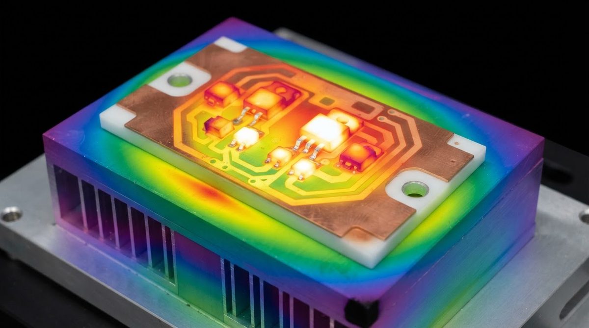
- Power semiconductor modules: IGBT, MOSFET, and SiC half-bridge modules from 600 V to 6.5 kV. The thick copper carries hundreds of amps; the ceramic provides galvanic isolation rated to several kV.
- High-power LED arrays: COB (chip-on-board) LED packages where die are soldered directly to the DBC copper.
- EV traction inverters: Si₃N₄ DBC substrates handle the extreme thermal cycling demanded by automotive qualification (per AQG 324).
- Industrial motor drives and welding equipment: Al₂O₃ DBC handles moderate power at lower cost.
When Not to Use a DBC Substrate
DBC is a power-electronics substrate, not a general-purpose PCB. Avoid it when:
- You need fine traces below 150 µm: DBC copper is thick and etched; minimum trace/space is typically 150–200 µm. For finer geometries, DPC (direct plated copper) or thin-film metallization is the right process.
- You need multilayer routing: DBC is a single-layer (or double-sided) technology. LTCC or hybrid stackups handle multilayer needs.
- Cost matters more than thermal performance: For dissipation below about 10 W/cm², a standard aluminum MCPCB at one-tenth the cost may be sufficient.
- Your application is RF: Thick DBC copper creates uncontrolled impedance at GHz frequencies. Thin-film on alumina or Rogers laminates are better choices.
DBC Substrate vs. AMB: What’s the Difference?
AMB (active metal brazing) is the main alternative high-power bonding method. Instead of an oxide eutectic, AMB uses a silver-copper-titanium braze alloy (e.g., Ag-Cu-Ti) at roughly 800–900 °C. The titanium reacts with the ceramic to form a strong bond.
AMB is required for Si₃N₄ substrates because Si₃N₄ does not form a stable oxide bond with copper at DBC temperatures. AMB also produces higher peel strength (typically > 8 N/mm) and better thermal-cycling endurance. The trade-off: AMB costs more and has longer cycle times. For Al₂O₃ and AlN at moderate cycling requirements, a DBC substrate remains the cost-effective default.
Frequently Asked Questions
Can I solder components directly to a DBC substrate?
Yes. The copper surface accepts standard solder alloys (SAC305, SnPb) and sintered silver. Surface finish is typically Ni/Au or bare copper with an OSP coating to prevent oxidation before soldering.
What is the maximum operating temperature for a DBC substrate?
The bond itself is stable well above 800 °C, but practical limits come from solder joints and die-attach materials. Most DBC power modules are rated to 150–200 °C continuous junction temperature. With sintered-silver die attach, operation up to 250 °C is feasible. See our guide on ceramic PCB frequently asked questions for more detail.
Does DBC work with silicon nitride ceramic?
Standard DBC does not bond reliably to Si₃N₄ because the oxide-eutectic mechanism requires a ceramic surface that wets well with Cu₂O. Si₃N₄ substrates use AMB (active metal brazing) instead. Products sometimes marketed as “Si₃N₄ DBC” are technically AMB.
How thick can the copper be on a DBC substrate?
Commercial DBC copper ranges from 0.127 mm (5 mil) to 0.635 mm (25 mil). Thicker copper carries more current and spreads heat laterally but increases CTE mismatch stress and limits etch resolution.
Is a DBC substrate the same as DPC?
No. A DBC substrate bonds bulk copper foil at high temperature. DPC (direct plated copper) sputters a thin seed layer and electroplates copper to 1–100 µm. DPC achieves finer traces (down to 20–50 µm) but carries far less current than DBC’s thick copper.