If you are asking what is AMB substrate, the short answer is this: an AMB (active metal brazing) substrate is a ceramic circuit board in which copper foil is bonded to a ceramic tile—typically Si₃N₄ or AlN—using a braze alloy containing an active element such as titanium. The titanium reacts with the ceramic surface to form a thin metallurgical bond strong enough to survive thousands of thermal cycles between −55 °C and +250 °C. AMB is the dominant substrate technology for SiC and IGBT power modules rated above 150 A.
Key Takeaways
- AMB uses a Ti-containing braze (commonly Ag-Cu-Ti) fired at 780–900 °C in vacuum to bond copper to ceramic.
- Peel strength of AMB joints typically exceeds 8 N/mm, versus 2–4 N/mm for DBC (direct bond copper).
- Silicon nitride (Si₃N₄) paired with AMB achieves >3 000 power cycles at ΔT = 175 K (per Kyocera SN-HPS datasheet), far exceeding Al₂O₃-DBC.
- Copper thickness on AMB substrates ranges from 0.3 mm to 1.5 mm, enabling high current-carrying capacity without wire bonds.
- AMB costs roughly 2–5× more than DBC per substrate, driven by vacuum brazing and Si₃N₄ ceramic pricing.
What Is AMB Substrate and How Does Active Metal Brazing Work?
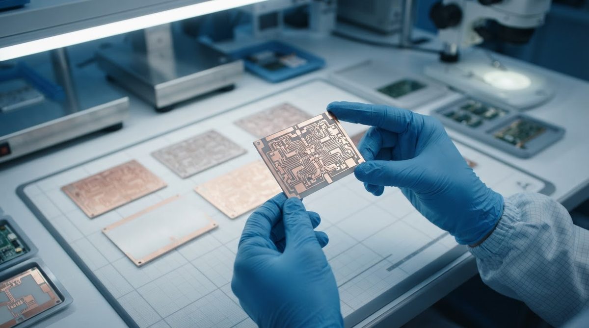
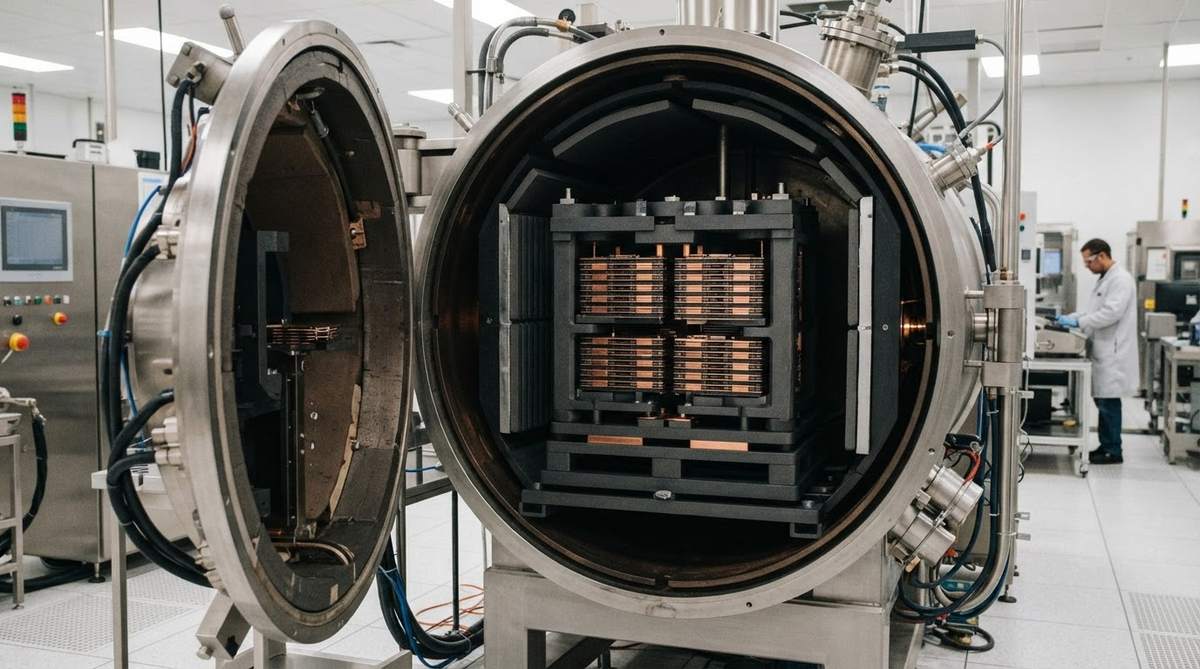
Standard brazing alloys do not wet oxide or nitride ceramics. AMB solves this by adding a small percentage of titanium (1.5–5 wt%) to a silver-copper eutectic alloy. During firing in a vacuum furnace (typically <10⁻³ Pa), the titanium diffuses to the ceramic interface and reacts to form TiN (on AlN) or TiN + Ti₅Si₃ (on Si₃N₄). This reaction layer is only 1–3 µm thick but converts the ceramic surface into something the molten Ag-Cu alloy can wet.
The process sequence is straightforward: (1) clean the ceramic tile and copper foils, (2) place braze foil or paste between them, (3) stack and fixture, (4) fire at 780–900 °C under vacuum for 10–30 minutes, (5) cool slowly to limit residual stress. After brazing, the copper is patterned by etching—the same photolithography-and-etch flow used for DBC. For details on that step, see how to etch copper on ceramic substrates.
Understanding what is AMB substrate at the process level helps explain why it outperforms DBC for thick-copper applications: the braze joint is a true metallurgical bond, not the oxide-mediated interface used in direct bonding.
AMB Substrate Properties
| Parameter | AMB on Si₃N₄ | AMB on AlN | Unit | Condition / Source |
|---|---|---|---|---|
| Ceramic thermal conductivity | 70–90 | 170–200 | W/mK | 20 °C; Kyocera SN-HPS / Maruwa AN-200 |
| Flexural strength (ceramic) | 600–900 | 300–400 | MPa | ASTM C1161; manufacturer datasheets |
| Fracture toughness (ceramic) | 6–7 | 2.5–3.5 | MPa·√m | ASTM C1421 |
| Copper thickness range | 0.3–1.5 | 0.3–0.8 | mm | Thinner Cu on AlN to limit CTE stress |
| Peel strength (Cu–ceramic) | 8–15 | 8–12 | N/mm | 90° peel test |
| Power-cycle life (ΔT = 175 K) | >3 000 | 800–1 500 | cycles | Kyocera SN-HPS / Heraeus published data |
| Max continuous use temp. | 300+ | 300+ | °C | Limited by braze alloy, not ceramic |
Typical values for commercially available material, for comparison only. Confirm against the datasheet for your specific grade.
The standout advantage of Si₃N₄-AMB is mechanical toughness. Silicon nitride’s fracture toughness (6–7 MPa·√m) is roughly double that of aluminum nitride (2.5–3.5 MPa·√m). That toughness lets the ceramic survive the stress imposed by thick copper during deep thermal cycling, which is why Si₃N₄-AMB dominates EV traction inverter modules.
Enter your substrate material, copper thickness, and operating temperature range below to see estimated derating behaviour for an AMB substrate configuration.
AMB vs. DBC: When Does the AMB Substrate Win?
| Criterion | DBC (Al₂O₃ or AlN) | AMB (Si₃N₄ or AlN) |
|---|---|---|
| Max practical Cu thickness | 0.3 mm (limited by oxide bonding) | 0.3–1.5 mm |
| Peel strength | 2–4 N/mm | 8–15 N/mm |
| Thermal-cycle reliability (ΔT > 100 K) | Moderate | High (especially on Si₃N₄) |
| Cost per substrate (relative) | 1× | 2–5× |
| Ceramic options | Al₂O₃, AlN, ZrO₂-toughened Al₂O₃ | Si₃N₄, AlN |
| Typical application | IGBT modules ≤150 A, LED | SiC/GaN modules, EV inverters, rail traction |
Sources: Heraeus Electronics technical literature; Rogers curamik product guide.
Choose DBC when junction temperatures stay below 150 °C, copper thickness ≤ 0.3 mm is sufficient, and cost matters more than cycle life. Choose an AMB substrate when any of these apply: SiC devices with junction temperatures above 175 °C, mission profiles with deep thermal swings (automotive, rail, wind), or current densities that demand copper thicker than 0.3 mm.
Worked Example: Why Thick Copper on an AMB Substrate Matters
Consider a half-bridge SiC module carrying 200 A continuous. Using the simplified DC current-carrying formula for a copper trace at 100 °C rise:
A 0.3 mm (300 µm) copper layer, 10 mm wide, has a cross-section of 3 mm². At a bulk resistivity of ~2.0 µΩ·cm (copper at 100 °C), its resistance over a 20 mm path is about 1.3 mΩ, dissipating roughly 52 W of I²R loss. Doubling the copper to 0.6 mm cuts that to ~26 W. At 1.2 mm copper—practical only with AMB—losses drop to ~13 W. In a 6-in-1 inverter module, that difference across all phases can shift total substrate losses by over 100 W, directly affecting coolant requirements.
When NOT to Use an AMB Substrate
AMB is overkill for LED thermal substrates, low-power sensor boards, and any design where junction temperature stays below 150 °C. In those cases, DBC on 96% alumina or even a metal-core PCB will meet the thermal and reliability requirements at a fraction of the cost. AMB also adds lead time: vacuum brazing runs are batch processes, and Si₃N₄ ceramic supply chains are tighter than Al₂O₃. If your prototype timeline is under four weeks, DBC is easier to source.
Frequently Asked Questions
Can I get AMB substrates on alumina (Al₂O₃)?
Technically yes—the braze alloy wets Al₂O₃—but it is rarely done. Alumina’s low fracture toughness (3–4 MPa·√m) limits copper thickness to about 0.3 mm before cracking risk rises, which eliminates AMB’s main advantage over DBC. Use DBC for alumina.
What braze alloys are used in AMB?
The most common is Ag-Cu-Ti (silver-copper eutectic with 1.5–4.5% titanium), sometimes called “Cusil-ABA” (Morgan Advanced Materials trade name). Variants with indium or tin exist for lower brazing temperatures. The alloy is supplied as foil (25–100 µm) or paste.
Does an AMB substrate support double-sided metallization?
Yes. Most power-module AMB substrates are brazed with copper on both sides in a single furnace run. The bottom copper serves as a base plate solder pad or direct heat-spreader interface.
Is AMB compatible with lead-free soldering?
Yes. Standard SAC305 reflow at 245–260 °C peak is well below the braze alloy’s solidus (~780 °C), so the joint is unaffected. Surface finishes such as Ni/Au or Ni/Ag are applied to the copper after etching to enable soldering.
How does an AMB substrate handle CTE mismatch with the die?
Si₃N₄ has a CTE of ~3.0 ppm/°C and AlN ~4.5 ppm/°C, both close to SiC (~4.0 ppm/°C) and Si (~2.6 ppm/°C). The thick copper layer (CTE ~17 ppm/°C) introduces mismatch, but the ceramic’s high toughness absorbs the resulting stress. Finite-element studies published by Infineon (PCIM Europe 2021) show Si₃N₄-AMB surviving >3 000 cycles at ΔT = 175 K without ceramic fracture.
Next Step
If you are evaluating ceramic substrates for a power module, start by comparing the full ceramic PCB FAQ for an overview of materials and processes. When you are ready to discuss your specific layout, request a quote with your Gerber files and thermal profile, and an engineer will review your design for manufacturability.