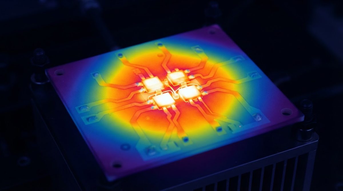
Aluminum nitride (AlN) conducts heat 6–8× better than 96% alumina (Al2O3)—170–200 W/m·K versus 24–28 W/m·K—but costs roughly 3–5× more per unit area in comparable substrate sizes. That single trade-off is the core of the alumina vs aluminum substrate decision. If your thermal budget closes with alumina, the cost savings are substantial. If it does not, AlN is usually the shortest path to a working design.
Key Takeaways
- 96% Al2O3 thermal conductivity is 24–28 W/m·K at 20 °C; AlN reaches 170–200 W/m·K under the same conditions (source: Kyocera, CoorsTek datasheets).
- AlN’s coefficient of thermal expansion (CTE) of 4.5–4.7 ppm/°C is a closer match to silicon (2.6 ppm/°C) than alumina’s 6.5–7.2 ppm/°C, reducing solder-joint fatigue in direct die-attach.
- Alumina is compatible with every major ceramic metallization process—DBC, DPC, AMB, HTCC, LTCC, thick film—while AlN is limited to DBC, DPC, AMB, and thin/thick film.
- Raw AlN substrates typically run $0.08–$0.20/cm² in volume versus $0.01–$0.04/cm² for 96% Al2O3, depending on size and thickness.
- For designs under roughly 30 W/cm² heat flux, 96% alumina often suffices; above that threshold, AlN or a redesign is usually necessary.
Alumina vs Aluminum Substrate: Property-by-Property Comparison
| Parameter | 96% Al2O3 | AlN | Unit | Condition | Source |
|---|---|---|---|---|---|
| Thermal conductivity | 24–28 | 170–200 | W/m·K | 20 °C | Kyocera SPC data, CoorsTek ADS-996 |
| CTE | 6.5–7.2 | 4.5–4.7 | ppm/°C | 20–300 °C | CoorsTek, Maruwa datasheets |
| Flexural strength | 340–380 | 300–350 | MPa | ASTM C1161, 3-pt bend | CeramTec, Kyocera |
| Dielectric constant (εr) | 9.4–9.8 | 8.5–9.0 | — | 1 MHz, 20 °C | Kyocera, Maruwa |
| Dielectric strength | 10–15 | 14–17 | kV/mm | AC, 60 Hz | CoorsTek |
| Loss tangent (tan δ) | 0.0002–0.0010 | 0.0003–0.0010 | — | 1 MHz | Kyocera |
| Density | 3.72–3.80 | 3.25–3.30 | g/cm³ | — | CoorsTek, Maruwa |
| Volume resistivity | >10¹⁴ | >10¹⁴ | Ω·cm | 25 °C | CeramTec |
| Max continuous use temp | 1600 | 1000 (in air) | °C | Oxidizing atmosphere | Kyocera, CoorsTek |
| Typical substrate cost | 0.01–0.04 | 0.08–0.20 | $/cm² | Volume, 0.635 mm thick | Industry pricing, 2024 |
Typical values for commercially available material, for comparison only. Confirm against the datasheet for your specific grade.
Two things stand out in the alumina vs aluminum substrate data. First, AlN’s thermal conductivity advantage is massive—not a marginal improvement but a category change. Second, alumina is mechanically slightly stronger and survives higher temperatures in oxidizing environments. AlN oxidizes above roughly 700 °C in air, forming an alumina surface layer that degrades thermal performance over time.
Thermal Performance: When Does the Alumina vs Aluminum Substrate Gap Matter?
A quick worked example puts numbers behind the choice. Consider a 10 × 10 mm substrate, 0.635 mm thick, dissipating 20 W uniformly from a die on one face to a heat sink on the other.
Thermal resistance through the substrate alone (Rth = t / (k × A)):
- 96% Al2O3: 0.000635 / (26 × 0.0001) = 0.244 °C/W → ΔT = 4.9 °C
- AlN: 0.000635 / (185 × 0.0001) = 0.034 °C/W → ΔT = 0.7 °C
At 20 W over 1 cm², the substrate-level temperature drop differs by only 4.2 °C. For many designs—LED modules, low-power sensor boards, RF hybrids below a few watts—that gap is irrelevant because the dominant thermal resistance sits at the die-attach or heat-sink interface, not the substrate itself.
Enter your own substrate area, thickness, and dissipated power below to estimate the junction temperature rise for each material.
Scale the power to 100 W over the same area (100 W/cm²), and the picture changes: alumina adds 24.4 °C while AlN adds 3.4 °C. At that flux, alumina may push junction temperature past its limit, and AlN becomes the practical choice. The crossover depends on your full thermal stack, but as a rough guideline, designs below 30 W/cm² should cost-check alumina first.
CTE Match to Silicon and Solder-Joint Reliability
Silicon’s CTE is about 2.6 ppm/°C. AlN at 4.5 ppm/°C sits closer to silicon than alumina at 6.5–7.2 ppm/°C. In direct die-attach with hard solder (AuSn, AuSi), that 2 ppm/°C gap matters during thermal cycling. A smaller CTE mismatch reduces shear stress in the solder layer and extends cycle life, per Coffin–Manson fatigue models.
For designs using soft solder (SAC305) or silver sintering with compliant bond lines, alumina’s higher CTE mismatch is more forgiving because the joint absorbs strain. If your assembly uses wire bonding to a packaged device rather than bare-die attach, CTE mismatch at the substrate level matters less, and alumina’s cost advantage wins.
Process Compatibility
Both substrates work with DBC and DPC metallization, but the process details differ.
DBC (Direct Bond Copper): Alumina DBC is the industry workhorse for power modules. AlN DBC requires a controlled-atmosphere furnace and tighter oxygen partial-pressure control during bonding, adding cost. Both yield copper layers of 0.127–0.50 mm.
DPC (Direct Plated Copper): Both substrates accept sputtered Ti/Cu seed layers followed by electrolytic copper build-up. DPC gives finer features (line/space down to 30–50 µm) than DBC, useful for high-density LED arrays or RF circuits.
AMB (Active Metal Brazing): AMB bonds copper to both alumina and AlN using a TiAgCu braze alloy at ~850 °C. DBC vs AMB process selection depends on copper thickness requirements and thermal-cycle targets. AMB on AlN is the standard for high-reliability IGBT modules (per Infineon and Wolfspeed application notes).
HTCC and LTCC: These co-fired processes use alumina-based tape systems. AlN is not processed via HTCC or LTCC in standard commercial production. If you need multilayer ceramic with embedded vias, alumina (or an HTCC vs LTCC comparison) is the path.
Cost Drivers and Practical Pricing
AlN’s cost premium comes from three places: raw material (AlN powder costs more than alumina powder), sintering (AlN requires nitrogen-atmosphere kilns and higher sintering temperatures around 1750–1900 °C), and yield (AlN is more sensitive to moisture and handling). Finished AlN substrates in production volumes typically cost 3–5× what equivalent alumina substrates cost.
Metallization cost is additive. An AlN DBC substrate might run 4–6× the price of an alumina DBC substrate of the same footprint, because the copper bonding step is also more expensive on AlN. For budget-constrained projects, it is worth checking whether a thinner alumina substrate (reducing Rth) or an alumina substrate with thermal vias can close the thermal gap before committing to AlN.
When NOT to Use AlN
Choose alumina over AlN when:
- Your thermal analysis shows the substrate is not the bottleneck—interface resistances or heat-sink performance dominate.
- You need multilayer co-fired structures (HTCC/LTCC). AlN is not available in these processes.
- The operating environment exceeds 700 °C in air. AlN oxidizes; alumina does not.
- Unit cost is the primary constraint and thermal performance is adequate with alumina.
When NOT to Use Alumina
Choose AlN over alumina when:
- Heat flux exceeds roughly 30 W/cm² and the thermal stack cannot tolerate the added resistance of alumina.
- Bare-die attach with hard solder requires a close CTE match to silicon or SiC.
- The application demands both high thermal conductivity and electrical isolation (AlN provides both; metal-core PCBs sacrifice isolation quality).
- If neither alumina nor AlN fits—perhaps you need extreme mechanical toughness under thermal cycling—consider AlN vs Si3N4 for power modules, where silicon nitride’s fracture toughness is roughly 3× that of AlN.
Decision Checklist
- Calculate substrate-level Rth for your actual die size, substrate thickness, and dissipated power.
- Compare that ΔT against your total thermal budget (junction limit minus ambient).
- If alumina ΔT fits within budget with margin, stop. Use alumina.
- If not, check whether a thinner alumina substrate, thermal vias, or a better heat-sink interface can recover the margin.
- If still short, specify AlN and budget accordingly.
- Verify your metallization process is compatible with the chosen substrate (especially for multilayer needs).
For designs where even AlN’s thermal conductivity is insufficient, or where beryllium oxide’s 250–300 W/m·K is considered, review the alumina vs beryllia substrate comparison—but note that BeO dust is a confirmed human carcinogen and carries significant handling, machining, and disposal restrictions.
Frequently Asked Questions
Can I solder components directly to both alumina and AlN substrates?
Yes, both substrates accept standard reflow soldering once metallized with copper (DBC, DPC, or AMB) and a solderable surface finish such as ENIG or Ni/Au. The bare ceramic itself is not solderable—metallization is required.
Does AlN degrade in humid environments?
Unprotected AlN hydrolyzes slowly in the presence of moisture, forming aluminum hydroxide on the surface. This is manageable: most AlN substrates are used in sealed modules or coated with a passivation layer. In open-air, high-humidity applications, alumina is more chemically stable without additional protection.
Is there a middle-ground material between alumina and AlN in thermal conductivity?
99.6% alumina reaches 28–35 W/m·K, a modest improvement over 96% alumina but still far below AlN. There is no widely available single ceramic that fills the 35–170 W/m·K gap at comparable cost. Silicon nitride (Si3N4) offers 70–90 W/m·K with superior fracture toughness, but it costs as much as or more than AlN. See the Si3N4 vs AlN comparison for details.
Which substrate is better for RF and microwave circuits?
Both work in RF applications, but alumina is far more common. Its dielectric constant (9.4–9.8 at 1 MHz) and loss tangent are well-characterized at microwave frequencies, and thin-film metallization on alumina is a mature process. AlN is used in RF only when thermal management of the active device demands it, such as GaN power amplifiers exceeding several watts per millimeter of gate width.
Do I need to change my PCB layout files when switching from alumina to AlN?
The layout geometry can remain identical if the substrate dimensions and metallization process stay the same. However, you should re-run impedance calculations because AlN’s lower dielectric constant (8.5–9.0 vs 9.4–9.8) changes characteristic impedance for transmission lines. Thermal via sizing may also change since AlN’s higher bulk conductivity reduces the need for via arrays.
Next Step
If you have settled the alumina vs aluminum substrate question for your project, the next step is to confirm that your chosen metallization process—DBC, DPC, or AMB—aligns with your trace geometry and copper thickness needs. Review the AMB vs DPC process comparison for guidance. When you are ready to get pricing on a specific substrate and process combination, request a quote from AluminaPCB.
Last reviewed: 2025-01.