This ceramic PCB comparison hub puts every major material, metallization process, and non-ceramic alternative side by side so you can narrow your shortlist in minutes instead of hours. No single ceramic option fits every project. The tables and decision forks below help you match your thermal, electrical, and cost requirements to the right substrate and process—then link out to the detailed head-to-head articles for deeper reading.
Ceramic Substrate Materials Compared
The substrate material determines thermal conductivity, dielectric strength, mechanical toughness, and cost. The table below covers the four materials you will encounter most often in ceramic PCB quotes.
| Parameter | Al₂O₃ 96% | Al₂O₃ 99.6% | AlN | Si₃N₄ |
|---|---|---|---|---|
| Thermal conductivity (W/mK, 20 °C) | 24–28 | 30–35 | 170–200 | 70–90 |
| Flexural strength (MPa, ASTM C1161) | 300–380 | 350–400 | 300–350 | 650–800 |
| Dielectric constant (1 MHz) | 9.0–9.5 | 9.7–10.0 | 8.5–9.0 | 8.0–9.0 |
| CTE (ppm/°C, 25–400 °C) | 7.0–7.5 | 7.2–7.8 | 4.3–4.7 | 2.5–3.5 |
| Max continuous use temp (°C) | ~1 600 | ~1 700 | ~1 000 (oxidation limit in air) | ~1 200 |
| Relative substrate cost (index) | 1× | 1.5–2× | 3–5× | 5–8× |
Typical values for commercially available material, for comparison only. Confirm against the datasheet for your specific grade. Sources: CoorsTek Advanced Ceramics datasheet; Kyocera Fine Ceramics catalog; Maruwa AlN substrate data.
Al₂O₃ 96% handles the majority of ceramic PCB projects because it balances thermal performance, machinability, and cost. When your thermal load outgrows alumina, AlN is the usual next step. Si₃N₄ is reserved for applications where mechanical shock or thermal cycling reliability matters more than raw conductivity—think power modules in EV inverters that see –40 °C to 175 °C swings. For a closer look at the two alumina grades, see the alumina 96% vs 99.6% substrate comparison.
Ceramic PCB Comparison Hub: Metallization Processes
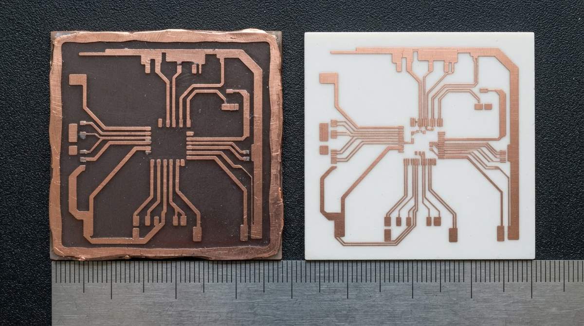
The metallization process bonds copper (or another conductor) to the ceramic. Each process imposes limits on trace resolution, copper thickness, and compatible substrates. This section of the ceramic PCB comparison hub covers the three dominant methods.
| Parameter | DBC | DPC | AMB |
|---|---|---|---|
| Full name | Direct Bond Copper | Direct Plated Copper | Active Metal Brazing |
| Copper thickness range | 150–600 µm | 1–200 µm | 200–800 µm |
| Min trace / space | ~200 µm / 200 µm | ~30 µm / 30 µm | ~250 µm / 250 µm |
| Compatible substrates | Al₂O₃, AlN | Al₂O₃, AlN | Al₂O₃, AlN, Si₃N₄ |
| Bond mechanism | Cu–O eutectic at ~1 065 °C | Sputtered Ti/Cu seed + electroplating | AgCuTi braze at ~800–900 °C |
| Thermal cycling reliability | Good | Good (thin Cu, less CTE stress) | Excellent (best for Si₃N₄) |
| Relative cost | Medium | Medium–High | High |
Typical ranges across multiple suppliers. Confirm with your manufacturer for specific capabilities.
DBC is the workhorse for power electronics on alumina or AlN when you need thick copper for high current. DPC wins when you need fine traces for RF or sensor layouts. AMB is the only reliable way to metallize Si₃N₄ and is increasingly specified for SiC power modules where thermal cycling counts exceed 10 000. Detailed breakdowns are available for DBC vs DPC, DBC vs AMB, and AMB vs DPC.
Ceramic PCB vs Non-Ceramic Alternatives
Not every thermal or high-frequency board needs ceramic. FR-4 and metal-core PCBs (MCPCBs) cover a large share of the market at lower cost. The question is where their limits become your problem. Use this part of the ceramic PCB comparison hub to see the gap in hard numbers.
| Parameter | Ceramic (Al₂O₃ 96%) | FR-4 | Aluminum MCPCB |
|---|---|---|---|
| Thermal conductivity (W/mK) | 24–28 | 0.25–0.35 | 1–4 (dielectric layer limited) |
| Max operating temp (°C) | 350+ (limited by solder/metallization) | 130 (Tg-dependent) | ~150 |
| Dielectric strength (kV/mm) | 15–20 | 20–40 | 4–8 (thin dielectric) |
| CTE (ppm/°C) | 7.0–7.5 | 14–17 (x/y) | 22–24 (aluminum) |
| Relative board cost (index, same area) | 5–15× | 1× | 1.5–3× |
Values representative of standard commercial grades. Confirm against supplier datasheets for your specific laminate or substrate.
The full cost picture is more nuanced than board price alone. For a total-cost-of-ownership analysis including rework, field failure, and heatsink savings, read the ceramic vs FR-4 cost comparison. If MCPCB is your main alternative, the ceramic vs MCPCB cost analysis breaks down where each technology is cheaper over a product’s lifetime.
Quick Decision Fork
Use this three-question filter to narrow your shortlist before requesting quotes:
- Is your junction-to-board thermal resistance budget below 1 °C/W for a 10 × 10 mm footprint? If yes, you likely need ceramic (AlN or at least Al₂O₃ 99.6%). FR-4 cannot get there, and MCPCB’s dielectric layer is the bottleneck.
- Does the board see continuous temperatures above 150 °C? If yes, FR-4 and standard MCPCBs are out. Ceramic or polyimide flex are your options.
- Do you need trace/space below 100 µm? If yes, specify DPC metallization. DBC and AMB cannot resolve features that fine.
If you answered “no” to all three, FR-4 or MCPCB probably meets your requirements at a fraction of the cost.
Enter your substrate material, thickness, and target power dissipation below to see estimated thermal resistance and temperature rise across each option in this ceramic PCB comparison hub.
When Not to Use Ceramic
Ceramic substrates are brittle, expensive, and limited in panel size (typically under 200 × 250 mm for alumina). Choose something else when:
- Your thermal load is under 5 W/cm² and ambient stays below 125 °C. Standard FR-4 with thermal vias or an aluminum MCPCB will work fine and cost 5–15× less per board.
- Your design needs mechanical flex or vibration damping. Ceramic fractures under bending loads that FR-4 or polyimide flex absorb easily.
- Board area exceeds roughly 150 × 200 mm and the full area needs metallization. Large ceramic panels are fragile to handle and expensive to fire. Consider tiling smaller ceramic substrates onto a metal baseplate instead.
- Your annual volume is above 100k units and the thermal requirement is moderate. At that scale, the cost premium of ceramic rarely pays back unless reliability in harsh environments is a regulatory requirement.
Worked Example: Choosing a Substrate for a 30 W LED Module
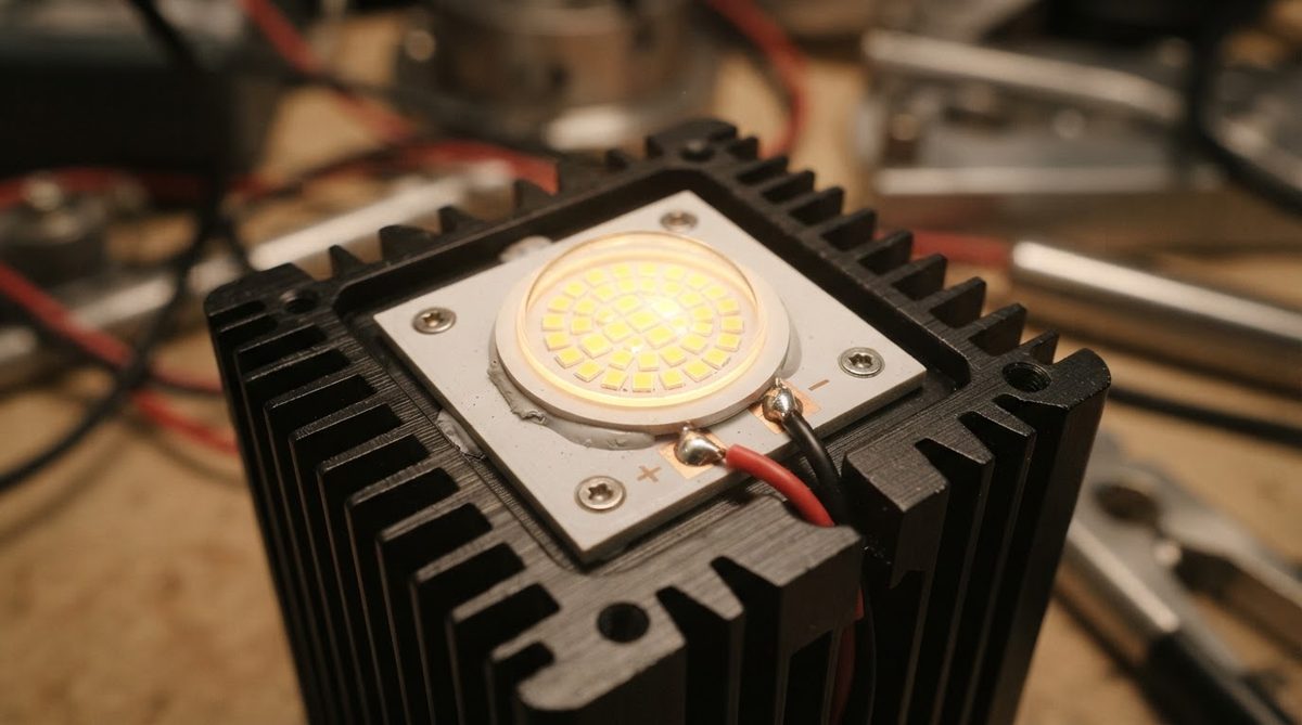
Suppose you have a 30 W COB LED array on a 25 × 25 mm footprint. The LED junction limit is 150 °C, ambient is 55 °C, and you need the board-level thermal resistance (θboard) to stay below 1.5 °C/W.
Thermal resistance through the substrate alone: θ = t / (k × A), where t is thickness, k is thermal conductivity, and A is area.
- FR-4 (1.6 mm, 0.3 W/mK): θ = 0.0016 / (0.3 × 0.000625) = 8.5 °C/W. Far too high.
- Al MCPCB (0.1 mm dielectric, 2 W/mK): θ = 0.0001 / (2 × 0.000625) = 0.08 °C/W. Passes, but the dielectric’s real bulk conductivity under copper pads is often closer to 1.5 W/mK, pushing θ to ~0.11 °C/W. Still passes, and costs much less.
- Al₂O₃ 96% (0.635 mm, 26 W/mK): θ = 0.000635 / (26 × 0.000625) = 0.039 °C/W. Passes with wide margin.
In this case, MCPCB is adequate thermally. Ceramic becomes the right call if you also need high-voltage isolation (the thin MCPCB dielectric may not withstand hipot testing above 2–3 kV) or if the module operates in an environment above 150 °C ambient.
Frequently Asked Questions
Can I mix ceramic and FR-4 in the same assembly?
Yes. A common approach is to mount a small ceramic substrate carrying the high-power or high-frequency components onto a larger FR-4 motherboard using solder or thermal adhesive. The CTE mismatch (7 vs 14–17 ppm/°C) must be managed with compliant interconnects or underfill.
Which ceramic material has the lowest cost per board?
Al₂O₃ 96% is the least expensive ceramic substrate, typically 3–5× the cost of equivalent-area FR-4 in prototype quantities. AlN and Si₃N₄ cost 3–8× more again than 96% alumina.
Is there a single ceramic PCB that works for both RF and power?
Rarely in one design. RF circuits favor thin substrates (0.25–0.38 mm) with DPC metallization for fine traces, while power circuits need thick copper (300 µm+) via DBC or AMB. Combining both on one substrate forces compromises on both sides. A hybrid approach with separate ceramic tiles is usually better.
How do I specify the right metallization process in my drawing?
Call out the copper thickness and minimum trace/space in your fabrication notes. If you need ≤100 µm lines, specify DPC. If you need ≥200 µm copper, specify DBC or AMB. Your fabricator can confirm compatibility with your chosen substrate material.
Does ceramic PCB need a solder mask?
It depends on the circuit density. Many ceramic boards use bare metallization with selective gold plating on bond pads instead of solder mask. For fine-pitch SMD layouts, a screen-printed glass or polymer overglaze can serve the same function as solder mask on FR-4.
Next Step
Pick the comparison most relevant to your project from the links above, or jump straight to a quote. Upload your Gerber files and substrate requirements, and the engineering team will recommend the material and process combination that fits your thermal, electrical, and cost targets.