DBC (Direct Bonded Copper) and AMB (Active Metal Brazing) are the two main processes for bonding copper foil to ceramic substrates used in power electronics. DBC relies on a copper-oxide eutectic formed at roughly 1065 °C to bond copper directly to Al₂O₃ or AlN. AMB uses a titanium-containing brazing alloy (typically AgCu-Ti) at around 850 °C to bond copper to Al₂O₃, AlN, or Si₃N₄. AMB handles thicker copper (up to 0.8 mm vs. DBC’s typical 0.3 mm limit), bonds reliably to Si₃N₄, and survives more thermal cycles — but it costs roughly 1.5–3× more than DBC for the same footprint.
Key Takeaways
- DBC is the established, lower-cost process for Al₂O₃ and AlN substrates carrying copper up to about 0.3 mm thick.
- AMB is required for Si₃N₄ substrates and for any design needing copper thicker than 0.3 mm on ceramic.
- AMB substrates survive 3,000+ thermal cycles (−40 °C to +150 °C) on Si₃N₄, versus roughly 800–1,500 cycles for DBC on Al₂O₃ (per Kyocera and Rogers published reliability data).
- DBC substrates dominate IGBT modules, while AMB on Si₃N₄ is becoming the baseline for SiC and GaN power modules where junction temperatures exceed 175 °C.
- Both processes are compatible with standard soldering, wire bonding, and sintered-silver die attach.
How DBC Bonding Works
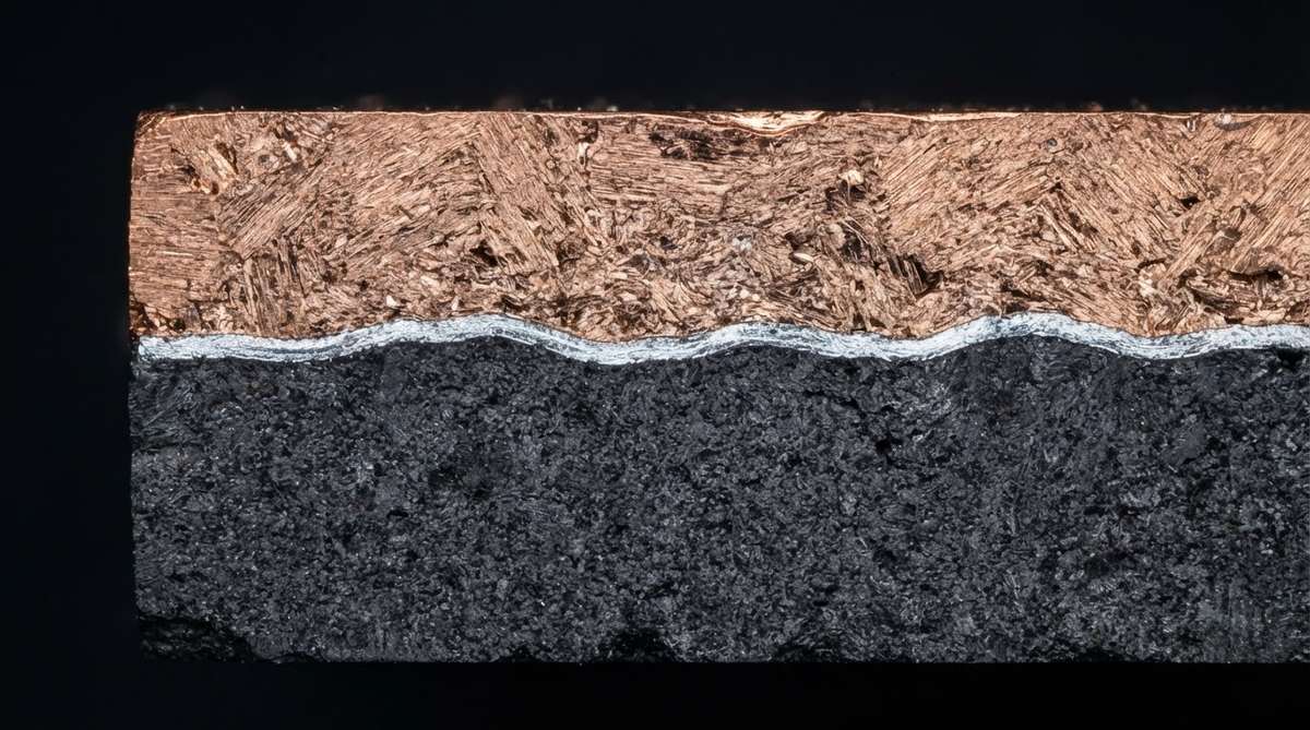
In DBC, oxygen is introduced into a furnace at approximately 1065 °C — just below the Cu-Cu₂O eutectic melting point of 1083 °C. A thin Cu₂O layer forms on the copper foil surface, melts, wets the ceramic, and solidifies into a direct oxide bond. The process works well on oxide ceramics (Al₂O₃) and, with a pre-oxidation step, on AlN.
Because the bond relies on the Cu-O eutectic, copper thickness is practically limited to about 0.3 mm. Thicker foils generate excessive CTE-mismatch stress during cool-down, causing ceramic cracking — especially on brittle Al₂O₃. Typical DBC copper is 0.127 mm (5 mil) to 0.3 mm (12 mil). Circuits are patterned by photolithographic etching after bonding.
DBC cannot reliably bond to Si₃N₄. The silicon nitride surface does not form the oxide interface DBC requires, and the high bonding temperature risks degrading the substrate. If your design specifies Si₃N₄, DBC is off the table.
How AMB Bonding Works
AMB places a thin brazing foil — usually Ag-Cu with 1–4 wt% titanium — between the copper foil and the ceramic. The stack is heated to around 820–880 °C in vacuum or inert atmosphere. Titanium in the alloy reacts with the ceramic surface to form a TiN or TiO₂ reaction layer, creating a chemical bond that is mechanically stronger than DBC’s oxide bond.
Because AMB operates roughly 200 °C below DBC’s bonding temperature, residual thermal stress after cool-down is lower. This allows thicker copper — up to 0.8 mm on Si₃N₄, and even 1.0 mm in some production lines — without cracking the ceramic. The braze layer itself is typically 10–25 µm thick and adds negligible thermal resistance (on the order of 0.01–0.02 K·cm²/W).
AMB bonds to all three common power-electronics ceramics: Al₂O₃, AlN, and Si₃N₄. It is the only volume-production process that reliably bonds copper to Si₃N₄. For a deeper comparison of Si₃N₄ versus AlN for power modules, see our dedicated guide.
DBC vs AMB: Head-to-Head Comparison
| Parameter | DBC | AMB | Unit / Condition | Source |
|---|---|---|---|---|
| Bonding temperature | ~1065 | 820–880 | °C | Rogers, Kyocera datasheets |
| Bonding atmosphere | N₂ + controlled O₂ | Vacuum or inert gas | — | Rogers curamik app note |
| Compatible ceramics | Al₂O₃, AlN | Al₂O₃, AlN, Si₃N₄ | — | — |
| Max practical Cu thickness | 0.3 | 0.8 (up to 1.0) | mm | Rogers, Toshiba Materials |
| Bond strength (peel) | 3–5 | 6–12 | N/mm | Kyocera SN series datasheet |
| Thermal cycles to failure (−40/+150 °C, Al₂O₃ 0.635 mm) | 800–1,500 | 1,500–3,000 | cycles | Rogers reliability report |
| Thermal cycles to failure (−40/+150 °C, Si₃N₄ 0.32 mm) | N/A | 3,000–10,000+ | cycles | Kyocera SN series datasheet |
| Relative cost (same footprint, Al₂O₃) | 1× | 1.5–2× | — | Industry pricing |
| Relative cost (Si₃N₄ substrate) | N/A | 3–5× vs DBC on Al₂O₃ | — | Industry pricing |
Typical values for commercially available material, for comparison only. Confirm against the datasheet for your specific grade.
Thermal Performance: A Worked Example
Consider a 25 mm × 25 mm substrate carrying a SiC MOSFET dissipating 150 W. We compare DBC on 0.635 mm AlN (170 W/mK) with AMB on 0.32 mm Si₃N₄ (90 W/mK), each with 0.3 mm copper on both sides.
Thermal resistance through the substrate stack
Rth = t / (k × A), where t is thickness, k is thermal conductivity, and A is area (6.25 × 10⁻⁴ m²).
- DBC / AlN: Ceramic contribution = 0.000635 / (170 × 6.25 × 10⁻⁴) = 0.006 K/W. Copper layers (2 × 0.3 mm, k = 390 W/mK) add 2 × 0.00077 = 0.0015 K/W. Total substrate Rth ≈ 0.0075 K/W → ΔT ≈ 1.1 °C at 150 W.
- AMB / Si₃N₄: Ceramic contribution = 0.00032 / (90 × 6.25 × 10⁻⁴) = 0.0057 K/W. Same copper layers add 0.0015 K/W. Braze layers (2 × 15 µm, k ≈ 200 W/mK) add ~0.0002 K/W. Total substrate Rth ≈ 0.0074 K/W → ΔT ≈ 1.1 °C at 150 W.
The numbers land nearly the same. Si₃N₄ has lower thermal conductivity, but its thinner standard dimension (0.32 mm vs. 0.635 mm) compensates. The real advantage of AMB/Si₃N₄ is mechanical: 3–10× more thermal cycles before failure, which matters in automotive and traction inverters where the substrate sees millions of power cycles over its lifetime.
When to Choose DBC
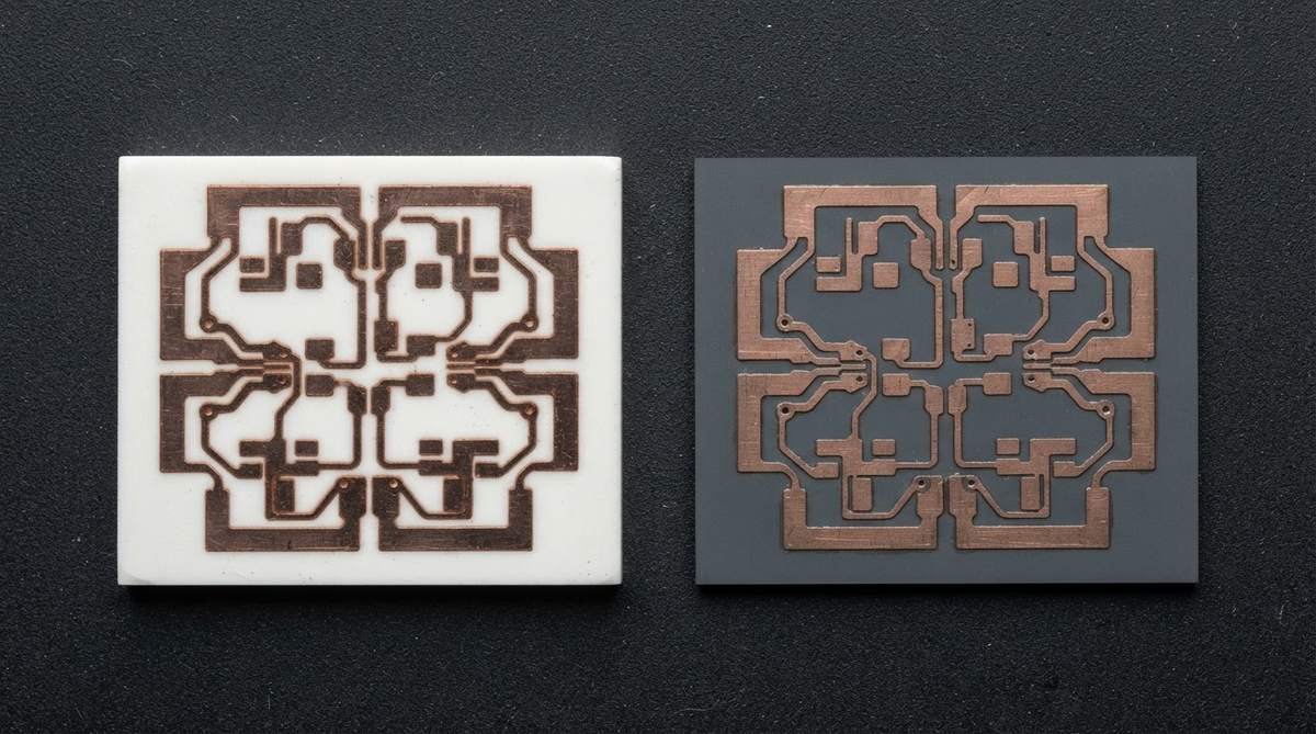
DBC is the right call when your design uses Al₂O₃ or AlN, copper thickness stays at or below 0.3 mm, and the thermal-cycling requirement is moderate — fewer than ~1,000 cycles at ΔT = 190 K. Standard IGBT modules for industrial drives, welding equipment, and UPS systems have used DBC on Al₂O₃ for decades with proven field reliability.
DBC is also simpler to source. More suppliers worldwide produce DBC substrates than AMB, and lead times are typically shorter. If your DBC versus DPC decision has already landed on DBC, and you do not need Si₃N₄ or thick copper, there is no reason to pay the AMB premium.
When to Choose AMB
Choose AMB when any of these conditions apply:
- Si₃N₄ substrate required. DBC cannot bond to it. Period.
- Copper thicker than 0.3 mm. High-current busbars integrated into the substrate, or designs needing low electrical resistance, benefit from 0.5–0.8 mm copper that only AMB can deliver.
- Severe thermal cycling. Automotive traction inverters (AEC-Q101 qualification typically demands 1,000+ cycles at −40/+175 °C), railway converters, and aerospace power stages all push beyond DBC’s reliable cycle count.
- SiC or GaN die with Tj,max above 175 °C. The higher junction temperatures and steeper thermal gradients of wide-bandgap devices generate more thermo-mechanical stress per cycle, favouring AMB’s stronger bond.
For designs comparing AMB against thinner metallization routes, our AMB versus DPC comparison covers trace resolution and cost trade-offs in detail.
When Not to Use Either DBC or AMB
If your power dissipation is under 5–10 W/cm² and the operating temperature stays below 150 °C, a metal-core PCB (MCPCB) at one-fifth the cost will usually suffice. For designs needing fine traces below 100 µm, DPC (Direct Plated Copper) or DPC and thin-film processes offer better resolution than the etched copper of DBC/AMB. And for RF or sensor substrates where metallization thickness is under 20 µm, thick-film or thin-film methods are more appropriate and far less expensive.
FR-4 remains the correct baseline for anything that does not specifically need ceramic’s thermal conductivity, CTE match, or high-temperature stability. Ceramic substrates solve real problems, but they are not a universal upgrade.
FAQ
Can I solder components to both DBC and AMB substrates?
Yes. Both DBC and AMB present a copper surface that accepts standard Sn-Ag-Cu (SAC) solder, high-temperature Au-Sn solder, and sintered-silver die attach. Surface finishes such as Ni/Au or Ni/Ag are applied the same way on either process.
Does the AMB braze layer create a significant thermal bottleneck?
No. The AgCu-Ti braze layer is typically 10–25 µm thick with a thermal conductivity around 200 W/mK. Its thermal resistance contribution is on the order of 0.01 K·cm²/W — negligible compared to the ceramic layer and the thermal interface material below the substrate.
Is AMB always better than DBC?
No. AMB costs 1.5–3× more, requires vacuum furnace processing, and has fewer global suppliers. For Al₂O₃-based modules with moderate cycling requirements, DBC delivers adequate reliability at lower cost and shorter lead time. Over-specifying AMB wastes budget.
Can I get DBC on Si₃N₄?
No. DBC requires a copper-oxide eutectic reaction with the ceramic surface, and Si₃N₄ does not support this bond chemistry. AMB is the only proven volume-production method for bonding copper foil to silicon nitride substrates.
What minimum trace width can I achieve with DBC or AMB?
Both processes use photolithographic etching of bonded copper foil. Minimum trace and space is roughly 150–200 µm for 0.3 mm copper, widening to 250–300 µm for 0.5 mm copper. Finer features require DPC or thin-film metallization instead.
Are DBC and AMB substrates RoHS compliant?
DBC substrates are inherently lead-free. AMB braze alloys based on Ag-Cu-Ti are also RoHS compliant. Some legacy braze formulations contained cadmium; confirm with your supplier that the specific alloy used is Cd-free and RoHS-listed.
Next Step
If you have settled on a ceramic bonding process and need substrates quoted, upload your design files for a ceramic PCB comparison and quote. For questions about substrate material selection, our Si₃N₄ vs AlN guide covers the ceramic side of the decision in detail.