When evaluating AMB vs DPC for ceramic substrates, the core trade-off is thick copper and brute endurance versus fine features and lower cost. Active metal brazing (AMB) bonds a thick copper foil (typically 127–800 µm) to the ceramic through a reactive Ti/Ag/Cu braze alloy fired at 780–900 °C, producing substrates that carry hundreds of amps and survive junction temperatures above 200 °C. Direct plated copper (DPC) sputters a thin adhesion/seed layer onto the ceramic and electroplates copper up to roughly 50–100 µm, achieving trace/space resolution as fine as 30–50 µm. Choose AMB when current capacity and thermal cycling endurance matter most; choose DPC when you need fine features, tight tolerances, or moderate power density at lower cost.
Key Takeaways
- AMB copper thickness ranges from 127 µm to 800 µm; DPC copper thickness typically spans 1 µm to 100 µm.
- DPC achieves minimum trace/space of 30–50 µm, roughly 5–10× finer than AMB’s practical limit of 200–300 µm.
- AMB substrates survive thermal cycling from −55 °C to +250 °C for thousands of cycles, per Kyocera and Rogers reliability data.
- DPC unit cost is typically 30–60% lower than AMB for equivalent substrate area, driven by simpler processing and thinner copper.
- In the AMB vs DPC decision, substrate material matters: AMB works on Al₂O₃, AlN, and Si₃N₄, while DPC works on Al₂O₃ and AlN but is most common on alumina.
How AMB vs DPC Processing Differs
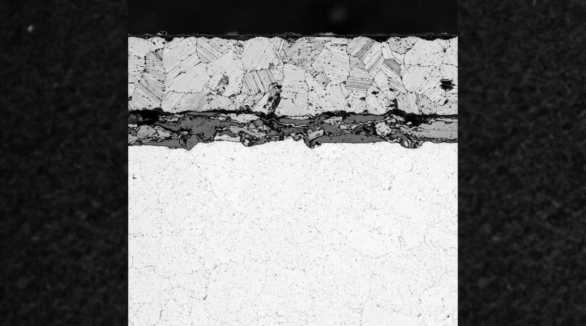
AMB (Active Metal Brazing)
A braze paste or foil containing an active metal—usually titanium—is placed between a pre-cut copper sheet and the ceramic substrate. The assembly enters a vacuum or inert-atmosphere furnace at 780–900 °C. Titanium reacts with the ceramic surface to form a thin TiN or TiO₂ interfacial layer that wets the ceramic, creating a chemical bond between the copper foil and the substrate. After brazing, circuits are patterned by etching the copper, similar to standard PCB processing. Because the copper starts as a solid foil, thicknesses of 300 µm or even 800 µm are routine. For a deeper look at how AMB compares with the older DBC eutectic method, see the DBC versus AMB comparison.
DPC (Direct Plated Copper)
The ceramic substrate is first cleaned and roughened (often by plasma or chemical treatment). A thin titanium or chromium adhesion layer (tens of nanometres) is sputtered onto the surface, followed by a copper seed layer of roughly 0.2–1 µm. Photoresist is applied and patterned, and copper is electroplated into the open areas to the target thickness—commonly 10–50 µm, sometimes up to 100 µm. After stripping the resist and etching the seed layer, the result is a high-resolution copper pattern bonded to the ceramic. DPC shares equipment and chemistry with semiconductor back-end processes, which is why its dimensional tolerances are tighter than foil-based methods. A related comparison of DBC and DPC substrates covers how DPC stacks up against the eutectic bonding route.
AMB vs DPC Specification Comparison
| Parameter | AMB | DPC | Unit | Notes / Source |
|---|---|---|---|---|
| Copper thickness range | 127–800 | 1–100 | µm | Rogers curamik / industry typical |
| Min trace / space | 200–300 | 30–50 | µm | After etch (AMB) / after plate-up (DPC) |
| Bond strength (peel) | ≥ 40 | 8–20 | N/cm | Per IEC 60249-2 peel test |
| Max continuous service temp | up to 300 | up to 300 | °C | Limited by ceramic, not copper bond |
| Thermal cycling endurance (−55/+250 °C) | > 3 000 cycles | 500–1 500 cycles | cycles | Kyocera reliability data (Si₃N₄ AMB) |
| Current-carrying capacity (1 cm trace) | 50–200+ | 5–20 | A | Depends on Cu thickness and cooling |
| Compatible ceramics | Al₂O₃, AlN, Si₃N₄ | Al₂O₃, AlN | — | Si₃N₄ AMB is standard for EV traction inverters |
| Typical unit cost (50 × 50 mm) | $8–$25 | $3–$10 | USD | Volume-dependent; indicative only |
| Lead time (prototype) | 4–8 weeks | 2–4 weeks | — | AMB requires vacuum furnace scheduling |
Typical values for commercially available material, for comparison only. Confirm against the datasheet for your specific grade.
Thermal Performance: A Worked Example
Consider a 10 × 10 mm die dissipating 50 W, mounted on a 1 mm-thick AlN substrate (thermal conductivity 170 W/mK) with copper on both sides. This example illustrates why the AMB vs DPC thermal gap is smaller than many engineers expect at the substrate level—but larger at the spreading level.
AMB case (300 µm Cu): Thermal resistance through the copper layer: R_Cu = t / (k × A) = 0.0003 m / (385 W/mK × 0.0001 m²) = 0.0078 K/W. Through the AlN: R_AlN = 0.001 / (170 × 0.0001) = 0.059 K/W. Total substrate stack ≈ 0.067 K/W. Temperature rise across the substrate: ΔT = 50 W × 0.067 = 3.3 °C.
DPC case (50 µm Cu): R_Cu = 0.00005 / (385 × 0.0001) = 0.0013 K/W. R_AlN stays the same at 0.059 K/W. Total ≈ 0.060 K/W. ΔT = 50 W × 0.060 = 3.0 °C.
The difference in substrate-level thermal resistance is small—about 0.007 K/W—because the AlN ceramic dominates. AMB’s advantage is not lower thermal resistance per se; it is the ability to spread heat laterally through thick copper before it enters the ceramic, which matters when the die is much smaller than the substrate. For a 3 × 3 mm die on a 25 × 25 mm substrate, the thick copper acts as an effective heat spreader, reducing hot-spot temperature by 10–20 °C compared to thin DPC copper, per Infineon application note AN2019-05.
When to Choose AMB
AMB is the default process for high-power modules: SiC and GaN traction inverters, IGBT modules rated above 100 A, and high-reliability aerospace converters. The thick copper handles surge currents that would fuse a DPC trace. The braze bond survives thousands of deep thermal cycles (−55 °C to +250 °C), which is critical for automotive-grade qualification per AQG 324. Si₃N₄ AMB substrates are now the standard in 800 V EV inverters because silicon nitride’s fracture toughness (6–7 MPa·√m per CoorsTek data) resists crack propagation under thermal stress far better than AlN (2.5–3.5 MPa·√m).
If your design requires wire-bonding pads larger than 5 mm² with pull strengths above 40 N/cm, or if you need to sinter silver paste onto the substrate at 250–300 °C, AMB’s thick, strongly bonded copper is the safer choice.
When to Choose DPC
DPC fits designs that need precision rather than brute current. Typical applications include LED driver substrates, RF front-end modules, sensor interposers, and MEMS packaging. The 30–50 µm trace/space capability lets you route dense patterns that AMB cannot achieve without laser trimming. DPC also pairs well with thin-film metallization in hybrid builds where some layers need resistor or capacitor integration.
Cost is the other driver. DPC skips the vacuum furnace step entirely, uses less copper, and processes on standard sputtering and plating lines. For mid-volume runs (500–5 000 pieces), expect 30–60% lower unit cost than AMB on the same substrate size. If your current per trace stays below roughly 10–15 A and your thermal cycling requirement is under 1 000 cycles, DPC delivers the performance you need at a fraction of the price.
When NOT to Use Either Process
If your design fits on FR-4 thermally and electrically, neither AMB nor DPC is justified. The cost premium is 5–20× per board. For moderate thermal loads (under 2 W/cm²) with no high-temperature or high-frequency requirement, a metal-core PCB (MCPCB) at 1–3 W/mK dielectric thermal conductivity is usually sufficient and far cheaper. See the ceramic versus FR-4 comparison for a fuller breakdown.
If you need thick copper AND fine traces on the same substrate, neither process alone covers both. Some manufacturers offer a hybrid approach—DPC fine features on one side, AMB power plane on the other—but this adds cost and complexity. For circuits where trace resolution below 10 µm is required (RF filters, precision thin-film resistors), look at thick-film versus thin-film processing instead.
AMB vs DPC Decision Checklist
Run through these five questions against your design. The answers point to the right process in the AMB vs DPC decision.
- Peak current per trace: Above 15 A → AMB. Below 15 A → DPC is likely sufficient.
- Minimum trace/space needed: Below 200 µm → DPC. Above 200 µm → either works.
- Thermal cycling requirement: Above 1 500 cycles at ΔT > 200 °C → AMB on Si₃N₄. Below 1 000 cycles → DPC on AlN or Al₂O₃ is acceptable.
- Budget sensitivity: If the substrate is more than 20% of your BOM and current/thermal requirements are moderate, DPC saves money.
- Substrate material: Si₃N₄ required → AMB (DPC on Si₃N₄ is not standard). Al₂O₃ or AlN → either process.
Frequently Asked Questions
Can you combine AMB and DPC on one substrate?
Yes, some fabricators offer hybrid builds with AMB on the power side and DPC fine lines on the control side. This adds a second metallization cycle and raises cost by roughly 40–80% over a single-process board. It is used mainly in integrated power modules where gate-driver traces sit on the same substrate as the power stage.
Does AMB work on alumina (Al₂O₃)?
AMB bonds reliably to 96% and 99.6% alumina, though it is most common on AlN and Si₃N₄. Alumina AMB substrates are less expensive but offer lower thermal conductivity (24–28 W/mK at 20 °C) than AlN (170–200 W/mK), so they suit medium-power applications where cost matters more than thermal resistance.
What surface finishes are available on DPC substrates?
DPC copper can receive the same finishes as conventional PCBs: ENIG, ENEPIG, OSP, immersion silver, and electroplated gold. ENIG is the most common for wire bonding. Finish selection depends on the assembly method—solder reflow, silver sintering, or ultrasonic wedge bonding each have different requirements.
Is AMB the same as DBC?
No. DBC (direct bonded copper) uses a copper-oxide eutectic reaction at ~1 065 °C to bond copper to the ceramic, with no braze alloy. AMB uses a reactive braze alloy containing titanium at 780–900 °C. AMB achieves stronger bonds on AlN and Si₃N₄ and survives more thermal cycles. The DBC vs AMB comparison page covers the differences in detail.
What is the maximum operating temperature for a DPC substrate?
The ceramic itself (Al₂O₃ or AlN) is stable well above 1 000 °C. The practical limit for a DPC substrate is set by the sputtered adhesion layer and the solder or die-attach material, typically 300–350 °C for continuous operation. Above that range, interdiffusion between Ti/Cu layers can degrade adhesion over time.
Next Step
If you have a power-module or sensor design and are unsure which metallization process fits, start by reviewing the ceramic PCB manufacturing process overview for broader context. When you are ready to get pricing on a specific substrate, request a quote with your Gerber files and copper-thickness requirements.