When comparing an alumina vs beryllia substrate, the headline difference is thermal conductivity: beryllium oxide (BeO) conducts heat roughly 7–10× better than 96% alumina — 250–300 W/mK versus 24–28 W/mK at 25 °C. But BeO is a serious inhalation hazard, costs 8–15× more per unit area, and faces tightening regulatory restrictions worldwide. For most ceramic PCB designs, 96% Al₂O₃ is the practical default; BeO is justified only when no other substrate can move enough heat in the available footprint.
Key Takeaways
- BeO thermal conductivity (250–300 W/mK per CoorsTek data) far exceeds 96% alumina (24–28 W/mK), but aluminum nitride (170–200 W/mK) closes much of that gap without the toxicity risk.
- Beryllium oxide dust is a confirmed human carcinogen (IARC Group 1) and causes chronic beryllium disease (CBD). Machining, grinding, and disposal require OSHA-regulated controls.
- 96% alumina substrates typically cost $0.30–$1.50 per cm² in volume; BeO substrates run $4–$15+ per cm² depending on size and purity.
- Both materials share similar dielectric constants (εr ≈ 6.5–6.8 for BeO, 9.0–9.5 for alumina at 1 MHz), so RF performance differences come mainly from loss tangent and surface finish, not permittivity.
- EU RoHS and REACH do not ban BeO outright, but downstream OEMs increasingly refuse it to avoid end-of-life disposal liability.
Alumina vs Beryllia Substrate: Property-by-Property Comparison
| Parameter | 96% Al₂O₃ | BeO (99.5%) | Unit | Condition | Source |
|---|---|---|---|---|---|
| Thermal conductivity | 24–28 | 250–300 | W/mK | 25 °C | CoorsTek / Materion datasheets |
| Dielectric constant (εr) | 9.0–9.5 | 6.5–6.8 | — | 1 MHz, 25 °C | Kyocera / Materion datasheets |
| Loss tangent (tan δ) | 0.0001–0.0004 | 0.0001–0.0003 | — | 1 MHz, 25 °C | Kyocera / Materion datasheets |
| Dielectric strength | 10–15 | 10–14 | kV/mm | ASTM D149 | CoorsTek |
| Flexural strength | 350–380 | 230–250 | MPa | ASTM C1161, 4-pt bend | CoorsTek / Materion |
| CTE | 7.2–8.0 | 7.5–8.5 | ppm/°C | 25–300 °C | CoorsTek / Materion |
| Max continuous use temp | 1 600 | 1 800 | °C | Inert atmosphere | CoorsTek / Materion |
| Density | 3.72–3.80 | 2.85–2.90 | g/cm³ | — | CoorsTek / Materion |
| Typical substrate cost | 0.30–1.50 | 4–15+ | $/cm² | Production volume | Industry estimates |
Typical values for commercially available material, for comparison only. Confirm against the datasheet for your specific grade.
For detailed alumina specifications, see the 96% Al₂O₃ substrate datasheet. Materion’s published BeO datasheets provide the corresponding beryllia figures; for a primer on the material itself, read beryllia material properties and hazard reference.
Thermal Conductivity: Where the Alumina vs Beryllia Substrate Gap Matters Most
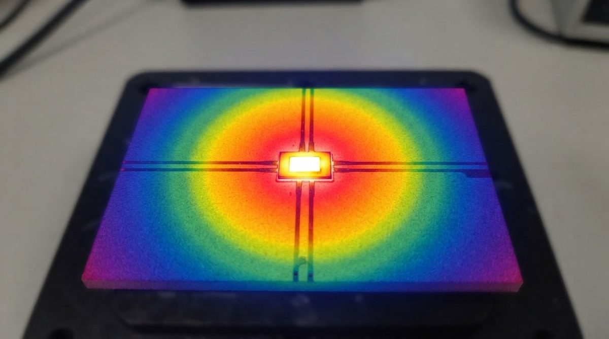
The thermal conductivity advantage of BeO over alumina is enormous. A 0.635 mm-thick BeO substrate under a 10 W die with a 5 × 5 mm footprint produces a conduction thermal resistance of roughly 0.085 °C/W (Rth = t / (k × A) = 0.000635 / (275 × 0.000025)). The same geometry in 96% alumina yields about 0.98 °C/W — more than 11× higher. That difference is the reason BeO historically dominated high-power microwave and radar modules.
Aluminum nitride (AlN, 170–200 W/mK) now fills much of that gap. In the same worked example, AlN gives roughly 0.15 °C/W. That is twice BeO’s resistance, but still 6× better than alumina, and it carries zero toxicity burden. For many power-amplifier and laser-diode applications, AlN has replaced BeO entirely since the early 2000s.
BeO still wins when the design needs the absolute lowest substrate thermal resistance in a constrained footprint — typically military radar T/R modules, certain TWT collectors, and legacy designs where the qualification baseline already specifies BeO.
Enter your substrate dimensions, material, and dissipated power below to estimate the conduction thermal resistance for each option in the alumina vs beryllia substrate comparison.
Beryllium Oxide Safety and Regulatory Concerns
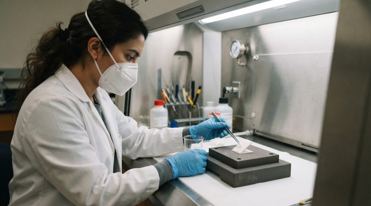
Beryllium oxide dust is a confirmed human carcinogen. Inhalation of BeO particles causes chronic beryllium disease (CBD), a progressive and incurable granulomatous lung condition. The hazard exists during machining, grinding, laser trimming, breakage, and disposal — any operation that generates dust or fumes from the fired ceramic. Intact, unbroken BeO substrates present minimal inhalation risk during normal handling, but downstream processes and end-of-life management remain regulated.
OSHA’s permissible exposure limit (PEL) for beryllium is 0.2 µg/m³ as an 8-hour TWA (29 CFR 1910.1024). Facilities that machine or solder BeO substrates must implement engineering controls, exposure monitoring, medical surveillance, and beryllium-specific waste handling.
From a regulatory standpoint, the EU REACH Candidate List includes beryllium compounds, and while fired BeO ceramic is currently exempt from RoHS substance restrictions, many European and Asian OEMs now prohibit it in new designs to avoid end-of-life disposal costs and supply-chain liability. U.S. defense programs remain the largest market for new BeO substrates.
Dielectric and RF Performance
BeO’s lower dielectric constant (6.5–6.8 vs 9.0–9.5 for 96% alumina at 1 MHz) means slightly wider transmission lines for a given impedance, which can ease fabrication tolerances at microwave frequencies. Loss tangent values are comparable — both materials are low-loss ceramics suitable for RF and microwave circuits through Ka-band and beyond.
For engineers choosing between thick-film and thin-film metallization on either substrate, the conductor loss in the metal layer typically dominates total insertion loss above 10 GHz. The substrate dielectric loss difference in the alumina vs beryllia substrate debate is measurable but rarely the deciding factor in a link budget.
Mechanical Strength and Handling
96% alumina is mechanically tougher than BeO. Its flexural strength (350–380 MPa, ASTM C1161) exceeds BeO’s (230–250 MPa) by roughly 40–60%. Alumina also tolerates more aggressive pick-and-place handling and wire bonding without fracture risk. BeO substrates require careful handling protocols — partly for mechanical reasons, partly because any chip or crack exposes fresh surface area that can generate hazardous dust.
Both materials have similar CTEs (7–8.5 ppm/°C), so CTE mismatch with silicon (2.6 ppm/°C) and GaN-on-SiC (4.5 ppm/°C) die is comparable. Neither substrate eliminates solder-joint fatigue in large-die attach, though BeO’s higher thermal conductivity reduces the thermal cycling amplitude the joint actually sees.
Cost and Supply Chain
BeO substrates are expensive by every measure. Raw beryllia powder costs more than alumina powder by roughly 20–30×. Only a handful of qualified suppliers worldwide produce fired BeO ceramics (Materion and a small number of specialty houses). Lead times of 12–20 weeks are common for custom BeO substrates, versus 2–6 weeks for standard alumina sizes.
If your design currently uses alumina and you need better thermal performance, AlN is the first alternative to evaluate. If your design currently uses BeO and you are looking to reduce cost or eliminate toxicity risk, AlN is again the most common drop-in candidate — though the 30–40% thermal conductivity reduction must be validated thermally. For standard alumina substrate dimensions and tolerances, see the 96% alumina thickness and tolerance options page.
When NOT to Use BeO
Do not specify BeO if any of the following apply:
- Your thermal analysis shows AlN (170–200 W/mK) provides adequate margin. Most new commercial designs fall into this category.
- Your product ships into the EU or Asian consumer markets where beryllium content triggers disposal or labeling obligations.
- Your facility lacks OSHA-compliant beryllium handling and waste controls.
- You need substrates in prototype quantities on short lead times — BeO supply is limited and slow.
- Your end product may be serviced in the field by personnel without beryllium-awareness training.
Conversely, do not assume 96% alumina is always sufficient. For power densities above roughly 50–80 W/cm² in a constrained footprint, alumina’s thermal resistance may force unacceptable junction temperatures. In those cases, evaluate AlN first, then BeO only if AlN cannot close the gap. For a broader substrate comparison, the ceramic vs FR-4 guide covers the jump from organic to ceramic materials.
Worked Example: Alumina vs Beryllia Substrate for a 25 W GaN PA
Consider a 25 W GaN HEMT die (3.2 × 1.6 mm) mounted on a 0.635 mm-thick substrate. The conduction thermal resistance through the substrate alone:
- 96% alumina: Rth = 0.000635 / (26 × 0.00000512) = 4.77 °C/W
- AlN: Rth = 0.000635 / (180 × 0.00000512) = 0.69 °C/W
- BeO: Rth = 0.000635 / (275 × 0.00000512) = 0.45 °C/W
At 25 W dissipation, the substrate-only ΔT is 119 °C for alumina, 17 °C for AlN, and 11 °C for BeO. The alumina option is likely disqualified. AlN and BeO both keep the substrate contribution well under 20 °C, so the choice between them depends on the total thermal stack, cost constraints, and regulatory requirements — not substrate thermal resistance alone.
Frequently Asked Questions
Is BeO banned under RoHS?
No. Fired beryllium oxide ceramic is not currently a restricted substance under EU RoHS Directive 2011/65/EU. However, beryllium compounds appear on the REACH Candidate List, and many OEMs voluntarily exclude BeO to avoid end-of-life disposal liability and supply-chain reporting obligations.
Can I replace BeO with AlN in an existing design?
In many cases, yes. AlN’s thermal conductivity (170–200 W/mK) is roughly 65–70% of BeO’s, so a thermal re-analysis is required. The CTE match to silicon and GaN die is actually better with AlN (4.5–5.0 ppm/°C) than with BeO (7.5–8.5 ppm/°C), which can improve solder-joint reliability.
What happens if a BeO substrate breaks during assembly?
A fractured BeO substrate generates fine ceramic dust that may contain respirable beryllium oxide particles. Work must stop, the area must be isolated, and cleanup must follow OSHA 29 CFR 1910.1024 procedures including HEPA vacuuming and wet wipe methods. Personnel in the area require medical evaluation per the beryllium standard.
Does BeO outperform alumina at RF frequencies?
BeO’s lower dielectric constant (6.5–6.8 vs 9.0–9.5) allows wider microstrip traces for a given impedance, easing fabrication. Loss tangent is similar for both materials. Above 10 GHz, conductor loss in the metallization typically dominates, so the substrate dielectric advantage of BeO is modest in most RF link budgets.
Where can I get BeO substrates?
Materion Corporation is the dominant Western supplier of fired BeO ceramics. A small number of specialty manufacturers in the U.S. and Japan also produce them. Lead times are typically 12–20 weeks for custom parts. AluminaPCB does not supply BeO substrates.
Next Step
If your alumina vs beryllia substrate analysis points toward 96% alumina or aluminum nitride rather than BeO, you can compare ceramic PCB substrate options and request a quote for prototypes or production quantities. For projects still in the material-selection phase, our engineering team can review your thermal stack and recommend the right substrate grade.