Aluminum nitride (AlN) is a ceramic substrate material with thermal conductivity of 170–200 W/mK (at 25 °C, per Kyocera SH-170 and Maruwa AN-200 datasheets), a coefficient of thermal expansion (CTE) of 4.4–4.7 ppm/°C that closely matches silicon (2.6 ppm/°C) and GaN (3.2 ppm/°C), and volume resistivity above 1014 Ω·cm. An aluminum nitride AlN PCB is the standard choice when a design must dissipate more than ~10 W/cm² through the substrate while maintaining reliable die attach and low dielectric loss at high frequency.
Key Takeaways
- AlN thermal conductivity (170–200 W/mK at 25 °C) is 6–8× higher than 96% alumina (24–28 W/mK) but costs 3–5× more per unit area.
- AlN CTE of 4.4–4.7 ppm/°C reduces solder-joint stress when bonding bare silicon or GaN die directly to the substrate.
- AlN substrates maintain a dielectric constant of 8.5–8.9 at 1 MHz (per ASTM D150) and a loss tangent below 0.001, making them viable for RF and mmWave carrier boards.
- Metallization options include DPC (sputtered Ti/Cu), DBC (direct-bonded copper), and thin-film processes; thick-film silver is less common due to AlN’s sensitivity to oxide-forming atmospheres.
- AlN is moisture-sensitive in powder form and requires nitrogen-atmosphere sintering, which drives both cost and lead time above alumina equivalents.
AlN Material Properties at a Glance
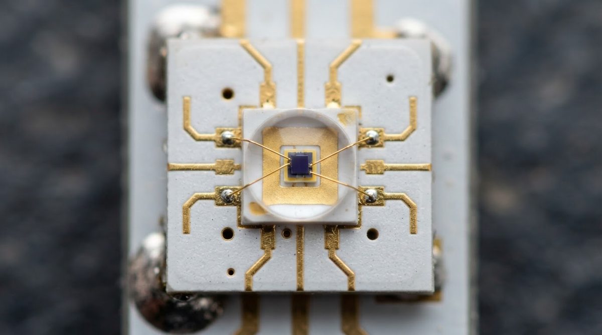
| Parameter | Value | Unit | Condition | Source |
|---|---|---|---|---|
| Thermal conductivity | 170–200 | W/mK | 25 °C | Kyocera SH-170 / Maruwa AN-200 datasheets |
| CTE | 4.4–4.7 | ppm/°C | 25–400 °C | Kyocera SH-170 datasheet |
| Dielectric constant (εr) | 8.5–8.9 | — | 1 MHz, 25 °C, ASTM D150 | Maruwa AN-200 datasheet |
| Loss tangent (tan δ) | < 0.001 | — | 1 MHz, 25 °C | Maruwa AN-200 datasheet |
| Volume resistivity | > 1014 | Ω·cm | 25 °C | CoorsTek ADS-996 datasheet |
| Flexural strength | 300–400 | MPa | 3-point bend, ASTM C1161 | Kyocera SH-170 datasheet |
| Dielectric strength | 14–17 | kV/mm | 25 °C | Maruwa AN-200 datasheet |
| Max. continuous use temp. | ~1000 | °C | In inert / N₂ atmosphere | CoorsTek technical bulletin |
| Density | 3.26 | g/cm³ | — | Kyocera SH-170 datasheet |
Typical values for commercially available material, for comparison only. Confirm against the datasheet for your specific grade.
For a full breakdown of grade-to-grade differences in thermal and electrical performance, see the AlN material properties reference.
How AlN Compares to Alumina and Si₃N₄
Engineers evaluating ceramic substrates usually narrow the field to three materials: 96% alumina (Al₂O₃), aluminum nitride (AlN), and silicon nitride (Si₃N₄). Each wins in a different scenario.
| Parameter | Al₂O₃ 96% | AlN | Si₃N₄ | Unit / Condition |
|---|---|---|---|---|
| Thermal conductivity | 24–28 | 170–200 | 70–90 | W/mK, 25 °C |
| CTE | 7.1 | 4.5 | 3.0 | ppm/°C, 25–400 °C |
| Flexural strength | 300–380 | 300–400 | 700–900 | MPa, ASTM C1161 |
| Fracture toughness (KIC) | 3.5–4.0 | 2.5–3.0 | 6.0–7.0 | MPa·m½ |
| Dielectric constant | 9.5–9.8 | 8.5–8.9 | 8.0–8.5 | 1 MHz |
| Relative substrate cost | 1× | 3–5× | 5–8× | Per unit area |
Sources: Kyocera, Maruwa, and CeramTec published datasheets. Values are typical midpoints for comparison only.
AlN wins on raw thermal performance. Si₃N₄ wins on mechanical toughness and thermal-shock resistance, which matters in power modules subjected to heavy thermal cycling (e.g., automotive inverters). Alumina wins on cost and availability. If your heat flux is below ~5 W/cm², alumina is usually sufficient. Use the comparison tool below to check the numbers against your own design constraints.
[pcb_calc type=”material-compare”]
A deeper look at how AlN dielectric constant affects high-frequency signal integrity is available separately.
Where AlN PCBs Are Used
High-Power LED and UV-C LED Modules
AlN’s thermal conductivity keeps junction temperatures low even at drive currents above 1 A. Its CTE match to GaN-on-sapphire die (sapphire ≈ 7.5 ppm/°C, GaN ≈ 3.2 ppm/°C) reduces interfacial stress. UV-C LEDs, which operate at wavelengths below 280 nm and generate significant waste heat in small die, are a particularly common application. More detail is in the guide to AlN PCBs for UV and UV-C LEDs.
RF and 5G mmWave Carrier Boards
A loss tangent below 0.001 at 1 MHz, combined with stable εr up to at least 10 GHz, makes AlN suitable for MMIC carriers and 5G front-end modules. The substrate’s high thermal conductivity also removes heat from GaN HEMT power amplifiers without requiring a separate heatsink. Engineers designing for 5G infrastructure frequently specify AlN for this dual benefit.
Power Electronics and SiC / GaN Modules
In SiC MOSFET and GaN HEMT modules, junction temperatures can exceed 200 °C. AlN DBC substrates handle continuous operating temperatures above 300 °C (limited by the metallization, not the ceramic). The CTE match to SiC (4.0 ppm/°C) keeps die-attach solder joints intact over thousands of thermal cycles.
Aerospace and Defence
Vacuum compatibility, radiation tolerance, and stable dielectric performance across a wide temperature range make AlN a standard substrate for space-qualified hybrid circuits. See the aerospace and defence AlN PCB guide for qualification considerations.
Worked Example: Thermal Resistance Through an AlN Substrate
Suppose you need to mount a 20 W GaN HEMT die (3 mm × 3 mm) on a 0.635 mm thick AlN substrate. The one-dimensional thermal resistance through the substrate is:
Rth = t / (k × A)
Where t = 0.635 × 10⁻³ m, k = 180 W/mK (mid-range AlN), A = 3 × 10⁻³ × 3 × 10⁻³ = 9 × 10⁻⁶ m².
Rth = 0.635 × 10⁻³ / (180 × 9 × 10⁻⁶) = 0.39 °C/W
For comparison, the same geometry in 96% alumina (k = 26 W/mK): Rth = 0.635 × 10⁻³ / (26 × 9 × 10⁻⁶) = 2.71 °C/W.
At 20 W dissipation, the temperature drop across the AlN substrate alone is 7.8 °C versus 54.2 °C for alumina. That 46 °C difference directly lowers junction temperature and extends device lifetime. For available AlN substrate thicknesses and tolerances, check the thickness options page.
Metallization and Surface Finish Options for AlN
AlN cannot be metallized the same way as alumina. Its surface oxidizes to form a thin Al₂O₃ layer, which actually helps adhesion in some processes but complicates others.
- DPC (Direct Plated Copper): Sputtered Ti/Cu seed layer followed by electroplated copper. Achieves line/space down to 50 µm. Best for fine-pitch RF circuits.
- DBC (Direct Bonded Copper): Copper foil bonded at ~1065 °C via a Cu–O eutectic. Typical copper thickness 0.15–0.30 mm. Suited to high-current power modules.
- Thin film (Ti/Pt/Au or Ti/Ni/Au): Deposited by sputtering or evaporation. Used for precision resistor networks and hybrid microelectronics.
- Thick film Ag/Pd: Possible but requires nitrogen-atmosphere firing to avoid AlN oxidation. Less common than on alumina.
Final surface finishes include ENIG, ENEPIG, electroplated Au, and immersion Ag. The right choice depends on the soldering method and the operating environment. Use the selector below to compare finish compatibility with your assembly process.
[pcb_calc type=”surface-finish”]
Surface roughness also matters for die attach and wire bonding. The AlN surface roughness guide covers Ra specifications for lapped and as-fired substrates.
Design Considerations Specific to AlN
Moisture Sensitivity
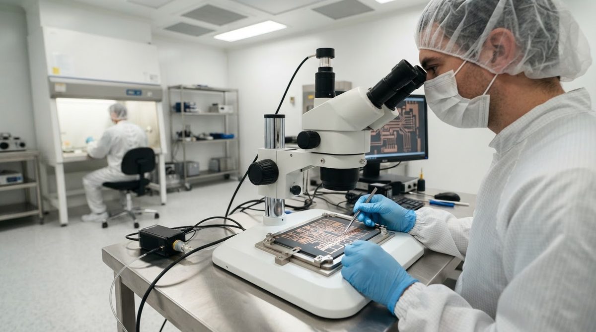
Bare AlN hydrolyzes slowly in humid environments, forming aluminum hydroxide on the surface. This degrades adhesion and changes surface resistivity over time. Most production substrates receive a thin oxidation layer (controlled surface Al₂O₃) during manufacturing that acts as a passivation barrier. Store unmetallized substrates in sealed, desiccated packaging.
Machining
AlN is harder to machine than alumina. Laser scribing (Nd:YAG or CO₂) is the standard method for scoring and singulation. Diamond grinding is used for edge profiling and via drilling. Mechanical punching is not practical. More on this topic at the AlN laser machining page.
CTE Matching
AlN’s CTE of 4.5 ppm/°C sits between silicon (2.6 ppm/°C) and copper (17 ppm/°C). This is an advantage for die attach but a challenge for thick copper metallization. DBC substrates with copper thicker than 0.3 mm may warp during thermal cycling. Designers should run a CTE mismatch stress analysis for any assembly that sees ΔT above 150 °C.
When Not to Use AlN
AlN is not the right substrate for every project. Choose something else in these situations:
- Heat flux below ~5 W/cm²: 96% alumina at one-third the cost will keep junction temperatures within spec. No point paying the AlN premium.
- Heavy thermal cycling with thick copper: Si₃N₄ (KIC 6–7 MPa·m½) survives many more thermal cycles than AlN (KIC 2.5–3.0 MPa·m½) in automotive power modules. If your spec calls for 3000+ power cycles at ΔT > 150 °C, evaluate Si₃N₄ first.
- Large-area, cost-sensitive boards: Metal-core PCBs (MCPCBs) with aluminum or copper bases are far cheaper per cm² and adequate for moderate thermal loads like LED lighting arrays.
- Standard digital or mixed-signal circuits: FR-4 or high-Tg FR-4 handles these at a fraction of the cost. Ceramic adds no value here.
- Prototype budgets under ~$500: Minimum order costs for AlN substrates with metallization typically start higher than this. Budget accordingly or start prototyping on alumina.
Sourcing AlN PCBs: What to Specify
When requesting a quote, include these items to avoid back-and-forth:
- AlN grade and purity: Standard commercial grades are ≥ 98% AlN. Higher purity (≥ 99%) pushes thermal conductivity toward 200 W/mK but increases cost. See the AlN grades comparison for specifics.
- Substrate dimensions and thickness: Common thicknesses are 0.25, 0.38, 0.50, and 0.635 mm. Thinner substrates reduce thermal resistance but are more fragile.
- Metallization type: DPC, DBC, or thin film. Include copper thickness if DBC.
- Surface finish: ENIG, ENEPIG, or electroplated Au. Specify plating thickness for wire-bond pads.
- Surface roughness (Ra): As-fired (~0.4–0.8 µm Ra) or lapped/polished (< 0.1 µm Ra).
- Quantity and schedule: AlN substrates have longer lead times than alumina. Plan for 3–5 weeks for prototypes.
Frequently Asked Questions
Can AlN substrates handle lead-free soldering temperatures?
Yes. AlN substrates are stable well above the 260 °C peak reflow temperature used in lead-free (SAC305) soldering. The ceramic itself is rated for continuous use above 800 °C. The limiting factor is the metallization and solder alloy, not the substrate.
Is AlN more fragile than alumina?
AlN has similar flexural strength (300–400 MPa vs. 300–380 MPa for 96% Al₂O₃) but lower fracture toughness (2.5–3.0 vs. 3.5–4.0 MPa·m½). In practice, AlN is slightly more prone to cracking from point impact or improper handling. Use vacuum pick-and-place tooling and avoid mechanical clamping on edges.
Does AlN work with wire bonding?
Yes, provided the surface finish supports it. Electroplated gold (≥ 1.5 µm) or thin-film Ti/Pt/Au pads are standard for both gold and aluminum wedge bonding. Surface roughness on bond pads should be below 0.2 µm Ra for consistent bond pull strength.
How does AlN perform at cryogenic temperatures?
AlN thermal conductivity increases significantly below room temperature, peaking around 50–70 K depending on purity. This makes AlN substrates useful in cryogenic sensor assemblies and superconducting electronics. CTE drops toward zero below 50 K, reducing thermal-cycling stress in cryo applications.
What is the shelf life of bare AlN substrates?
Stored in sealed, desiccated packaging at room temperature, bare AlN substrates remain usable for at least 12 months. Prolonged exposure to humid air causes surface hydrolysis. If substrates have been stored open, a light surface etch or plasma clean before metallization restores adhesion.
Can I get AlN substrates with vias?
Yes. Vias in AlN are typically laser-drilled and filled with tungsten or copper paste, then co-fired or plated. Minimum via diameters of 0.1–0.15 mm are achievable with laser processing. Filled vias provide thermal and electrical paths through the substrate for double-sided designs.
Next Step
If your thermal analysis points to AlN, the next move is to lock down the grade, thickness, and metallization type. Download the AlN substrate datasheet for detailed property data, or submit your design files for a quote at custom AlN PCB fabrication.