Aluminum nitride AlN surface roughness spans roughly Ra 0.3–1.0 µm in the as-fired condition and can be reduced to Ra 0.025 µm or below with mechanical lapping and chemical-mechanical polishing (CMP). The finish you specify determines metallization adhesion strength, wire-bond yield, thermal interface resistance, and cost. Most power-electronics and RF projects land on one of three grades: as-fired, lapped, or polished.
Key Takeaways
- As-fired AlN substrates typically measure Ra 0.3–1.0 µm, suitable for thick-film printing and DBC bonding.
- Lapped AlN reaches Ra 0.1–0.25 µm, the minimum most thin-film sputtering processes require for reliable adhesion.
- Polished (CMP) AlN can hit Ra 0.025 µm or lower, needed for sub-micron thin-film features and optical applications.
- Every step from as-fired to polished roughly doubles substrate cost per unit area.
- Aluminum nitride AlN surface roughness also affects thermal interface resistance: a smoother surface reduces contact resistance at die-attach and heat-sink interfaces.
How Aluminum Nitride AlN Surface Roughness Is Measured
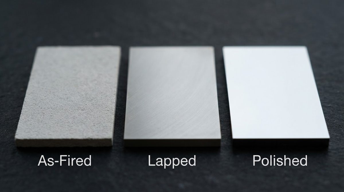
Surface roughness on AlN substrates is reported as Ra (arithmetic average roughness) per ISO 4287 or ASME B46.1. A stylus profilometer or white-light interferometer scans a defined evaluation length and calculates the mean deviation from the centerline. Suppliers may also report Rz (average peak-to-valley height), which is typically 4–6× the Ra value for sintered ceramics.
When comparing datasheets, confirm the measurement method and evaluation length. A Ra figure from a 0.8 mm cutoff length is not directly comparable to one from a 2.5 mm cutoff. Kyocera, Maruwa, and CoorsTek all publish AlN roughness data using ISO 4287 with a 0.8 mm cutoff as the default, so cross-supplier comparison is usually straightforward if you stick to those brands.
AlN Surface Roughness by Finish Grade
| Finish grade | Typical Ra (µm) | Typical Rz (µm) | Primary use | Relative cost |
|---|---|---|---|---|
| As-fired | 0.3–1.0 | 2.0–6.0 | DBC, thick-film printing, general assembly | 1× |
| Lapped (ground) | 0.1–0.25 | 0.8–1.5 | Thin-film sputtering, high-frequency circuits | ~1.5–2× |
| Polished (CMP) | 0.01–0.05 | 0.05–0.3 | Sub-micron thin-film features, optical, MEMS | ~2.5–4× |
Typical values for commercially available AlN (≥ 98% purity, 170–200 W/mK), for comparison only. Confirm against the datasheet for your specific grade.
Why Aluminum Nitride AlN Surface Roughness Matters for Metallization
Thin-film processes (sputtering, evaporation) deposit metal layers measured in hundreds of nanometers. If the substrate Ra approaches or exceeds the metal layer thickness, the film develops discontinuities, pinholes, and poor step coverage over grain peaks. For a 200 nm Ti/Pt/Au stack, you generally need Ra below 0.2 µm. For a 5 µm thick-film screen print, Ra up to 0.8 µm is workable.
Adhesion pull strength also correlates with roughness, but the relationship is not linear. A moderately rough surface (Ra 0.15–0.25 µm) can actually outperform a mirror polish because mechanical interlocking supplements chemical bonding. Going below Ra 0.05 µm is only justified when feature geometry demands it or when you need extremely low RF loss at frequencies above 30 GHz.
Worked Example: Thin-Film Adhesion Budget
Suppose you are sputtering a 150 nm TiW / 3 µm Cu stack for a 77 GHz radar substrate. The Cu skin depth at 77 GHz is approximately 0.75 µm. Surface peaks taller than about one-third of the skin depth (≈ 0.25 µm) scatter current and increase insertion loss. With as-fired AlN at Ra 0.6 µm (Rz ≈ 3.5 µm), the peak-to-valley excursions far exceed this threshold. Lapping to Ra 0.15 µm (Rz ≈ 1.0 µm) brings the peaks within budget. Polishing to Ra 0.03 µm would further reduce loss by an estimated 0.02–0.05 dB/cm at 77 GHz, but at 2–3× the substrate cost. For most automotive radar applications, lapped finish is the practical sweet spot.
Effect on Thermal Interface Resistance
At a bare ceramic-to-heat-sink interface with thermal grease, contact thermal resistance drops as aluminum nitride AlN surface roughness decreases. A simple model from Cooper, Mikic, and Yovanovich (1969) estimates contact resistance as proportional to (Ra₁ + Ra₂) / k_grease. Reducing AlN Ra from 0.8 µm to 0.15 µm can cut the grease-layer contribution by roughly 40%, assuming the mating surface stays constant. For a 10 × 10 mm die dissipating 50 W, that translates to approximately 0.5–1.0 °C lower junction temperature — meaningful in high-reliability designs but negligible for most commercial products.
If thermal contact is your primary concern, a lapped finish paired with a well-chosen thermal interface material often outperforms a polished finish with a cheap grease. Spend the budget on the right TIM before upgrading to CMP polish.
Comparing AlN Roughness to Other Ceramic Substrates
[pcb_calc type=”material-compare”]
| Substrate | As-fired Ra (µm) | Best achievable Ra (µm) | Thermal conductivity (W/mK) | Source |
|---|---|---|---|---|
| AlN (≥ 98%) | 0.3–1.0 | 0.01–0.05 | 170–200 (at 20 °C) | Kyocera SH-170 datasheet |
| Al₂O₃ 96% | 0.4–1.2 | 0.02–0.05 | 24–28 (at 20 °C) | CoorsTek ADS-96R datasheet |
| Si₃N₄ | 0.3–0.8 | 0.02–0.04 | 70–90 (at 20 °C) | Maruwa SN-90 datasheet |
Typical values for commercially available material, for comparison only. Confirm against the datasheet for your specific grade.
AlN and alumina reach similar polished finishes because both are fine-grained polycrystalline ceramics. Silicon nitride polished substrates also achieve comparable Ra values but with higher fracture toughness, making them easier to handle during lapping. For thermal performance, AlN remains the strongest option among oxide and nitride ceramics at this roughness level. If you are evaluating AlN thin substrates below 0.25 mm, note that lapping very thin pieces increases breakage rates and cost.
How Purity Affects Achievable AlN Surface Roughness
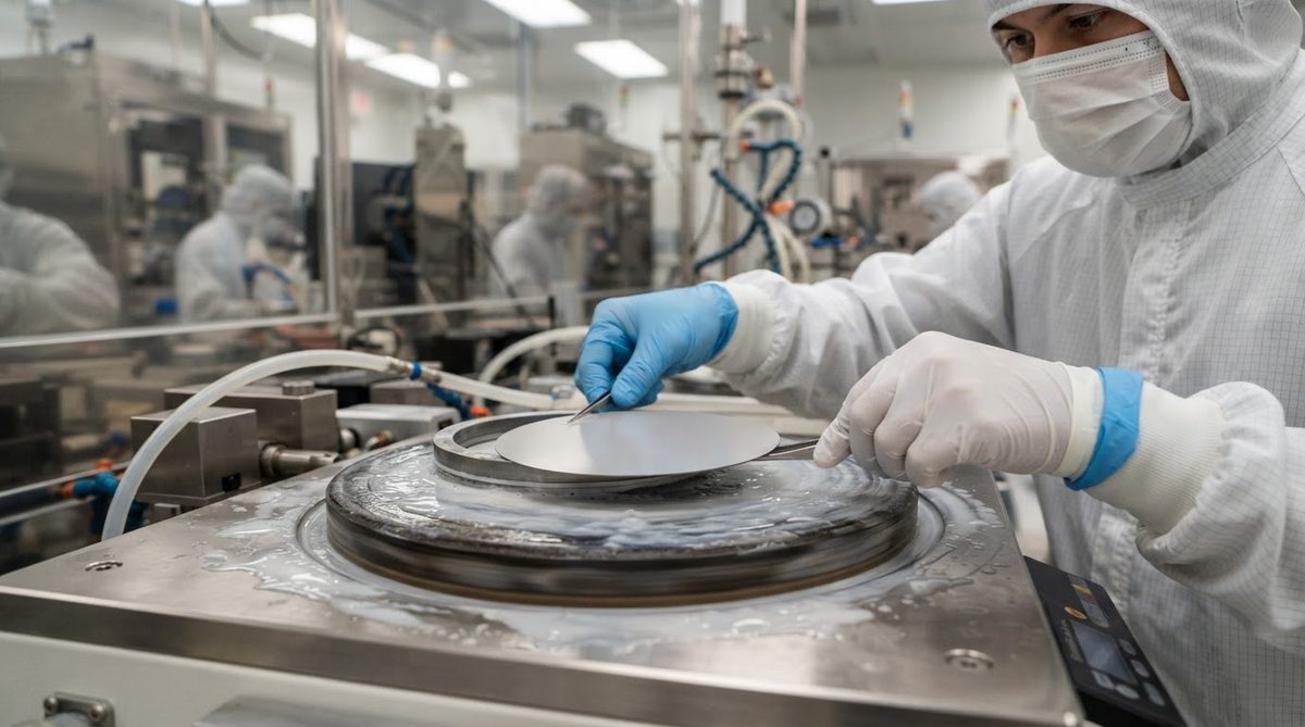
AlN substrates with higher purity (≥ 99%) have finer, more uniform grain structure — typically 2–5 µm grain size versus 5–10 µm for 95% purity grades. Finer grains mean fewer large surface asperities after sintering and faster convergence during lapping. If your process demands Ra below 0.1 µm, specify ≥ 98% purity AlN. Lower-purity grades may never reach that target without excessive material removal. For a deeper discussion of how composition drives substrate performance, see how purity affects ceramic substrate performance.
When Not to Specify a Polished AlN Surface
Polished AlN is overkill — and a waste of budget — in several common scenarios:
- DBC (direct bond copper) substrates: The copper bonding process itself creates a new surface. As-fired Ra 0.5–0.8 µm is standard for DBC.
- Thick-film circuits: Screen-printed pastes fill surface valleys. Ra up to 0.8 µm is acceptable.
- Structural or heater applications: If no metallization is applied, surface finish is cosmetic unless it affects sealing or mating surfaces.
- Cost-sensitive power modules: Lapped finish at Ra 0.15–0.2 µm covers most sputtered metallization needs at half the cost of CMP.
If your thermal conductivity requirements are below 90 W/mK, alumina or silicon nitride PCBs may be more cost-effective substrates to polish, since the raw material is cheaper.
Specifying Aluminum Nitride AlN Surface Roughness on a Drawing
Call out Ra (not Rz alone) with the measurement standard, cutoff length, and evaluation length. A clear callout looks like this:
Surface finish: Ra ≤ 0.20 µm per ISO 4287, λc = 0.8 mm, ln = 4.0 mm, both sides.
Specify “both sides” if metallization or thermal contact occurs on each face. If only one side matters, say so — lapping a single side cuts processing time and cost. Also state whether edge chamfers or laser-scribed features are included in the roughness spec, because those areas will have different Ra values.
FAQ
Can I get AlN substrates smoother than Ra 0.01 µm?
Yes, but it requires extended CMP processing and is typically reserved for optical or MEMS applications. Expect lead times 2–3× longer and significant cost premiums. Most electronics applications do not benefit below Ra 0.025 µm.
Does lapping AlN change its thermal conductivity?
No. Lapping removes only 10–50 µm of surface material. The bulk thermal conductivity (170–200 W/mK for ≥ 98% purity) is unchanged. Surface micro-cracking from aggressive grinding could theoretically increase local thermal resistance, but this is avoided with proper process control.
What Ra do I need for gold wire bonding directly to metallized AlN?
The substrate Ra matters only indirectly — what counts is the metallization surface roughness. A sputtered Au pad on lapped AlN (Ra ≤ 0.2 µm) typically presents a bonding surface of Ra 0.05–0.1 µm, well within the range for reliable thermosonic ball bonding per MIL-STD-883 Method 2011.
Is as-fired roughness consistent across different AlN suppliers?
Not always. As-fired Ra depends on powder particle size, sintering temperature, and sintering aid chemistry. Two suppliers both calling their product “AlN 98%” may deliver Ra 0.4 µm and Ra 0.9 µm respectively. Always request an aluminum nitride AlN surface roughness spec on the purchase order, not just a purity grade.
How do I choose between AlN and Si₃N₄ when both need polishing?
Choose AlN when thermal conductivity above 150 W/mK is required. Choose the right ceramic substrate based on mechanical robustness if your design involves thermal cycling or mechanical shock — Si₃N₄ has roughly 3× the fracture toughness of AlN, making it far more resistant to cracking during handling and assembly.
Next Step
If you have a target Ra and substrate thickness in mind, request a quote with your roughness spec included. Pricing varies significantly by finish grade, and AlN wholesale pricing improves at volumes above 100 pieces for lapped or polished grades.