Aluminum nitride AlN laser machining is the preferred method for cutting, drilling, and scribing AlN substrates used in ceramic PCBs. AlN is too hard (Vickers hardness ~1,000 HV) and too brittle for conventional mechanical routing, so CO₂ and UV-wavelength lasers handle the bulk of subtractive processing. Typical positional tolerances land in the ±25–50 µm range, with kerf widths of 30–100 µm depending on wavelength and beam optics.
Key Takeaways
- CO₂ lasers (10.6 µm) cut AlN substrates up to ~1.0 mm thick efficiently, but leave a wider heat-affected zone (HAZ) of 50–150 µm.
- UV lasers (355 nm Nd:YAG or 248 nm excimer) produce a HAZ under 20 µm and kerf widths of 20–40 µm, suitable for fine features.
- Laser scribing followed by mechanical snap is the fastest, lowest-cost method for panel singulation.
- Post-machining surface roughness in the cut zone typically ranges from Ra 1.0–3.0 µm; lapping or polishing is needed if Ra < 0.5 µm is required on cut edges.
- AlN absorbs 10.6 µm wavelength radiation strongly, which is why CO₂ lasers work well despite being a thermal process.
Why Aluminum Nitride AlN Laser Machining Is the Default Process
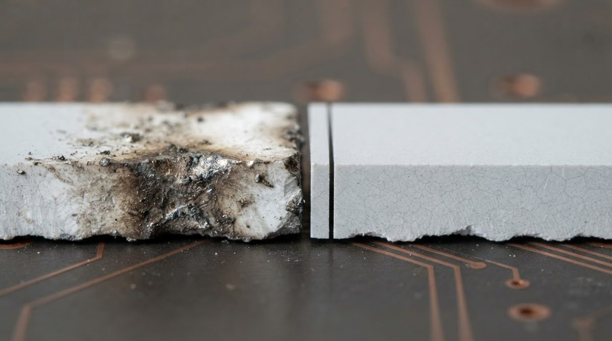
Aluminum nitride has a thermal conductivity of 170–200 W/mK (per Kyocera and Maruwa datasheets, measured at 25 °C) and a flexural strength of 300–400 MPa (ASTM C1161 four-point bend). The high hardness means diamond-blade dicing wears tooling fast and generates micro-cracks along cut edges. Water-jet cutting introduces moisture that can degrade unpassivated metallisation. Lasers avoid mechanical contact entirely, eliminating crack propagation from tool pressure.
AlN also has a relatively high absorption coefficient at the CO₂ wavelength (10.6 µm), which means most of the beam energy couples directly into the material rather than reflecting. This makes the process energy-efficient compared to laser-cutting alumina, where higher reflectance at certain wavelengths can slow throughput.
Wavelength Selection for AlN Laser Machining: CO₂ vs. UV vs. Fibre
The choice of laser wavelength determines HAZ size, edge quality, and throughput. Each wavelength interacts with AlN differently.
| Parameter | CO₂ (10.6 µm) | UV Nd:YAG (355 nm) | Fibre (1.06 µm) |
|---|---|---|---|
| Typical kerf width | 60–100 µm | 20–40 µm | 40–70 µm |
| HAZ width | 50–150 µm | 5–20 µm | 30–80 µm |
| Cut-edge roughness (Ra) | 1.5–3.0 µm | 0.5–1.5 µm | 1.0–2.5 µm |
| Max practical thickness | ~1.0 mm single pass | ~0.38 mm (multi-pass) | ~0.63 mm |
| Relative throughput | High | Low | Medium |
| Relative cost per part | Low | High | Medium |
Typical values for commercially available equipment; actual results depend on beam quality (M²), pulse duration, and assist-gas setup. Confirm against your laser vendor’s process data.
For most PCB-scale aluminum nitride AlN laser machining tasks—panel singulation, via drilling, and alignment-hole cutting—CO₂ lasers offer the best balance of speed and cost. UV lasers are justified when feature tolerances drop below ±25 µm or when the HAZ must stay under 20 µm, such as near wire-bond pads. Fibre lasers at 1.06 µm are less common for AlN because absorption at that wavelength is lower, requiring more passes and generating more re-deposited debris.
Critical Process Parameters
Four variables control cut quality more than anything else during aluminum nitride AlN laser machining: pulse energy, repetition rate, feed speed, and assist gas.
Pulse Energy and Repetition Rate
Higher pulse energy removes more material per pulse but drives up HAZ width. For a CO₂ laser cutting 0.635 mm AlN, a typical starting point is 8–12 W average power, 5–20 kHz repetition rate, with a feed speed of 10–30 mm/s. UV lasers operate at much lower average power (1–5 W) but pulse energies of 50–200 µJ at 10–50 kHz.
Assist Gas
Nitrogen or clean dry air blown coaxially with the beam clears molten debris from the kerf and suppresses oxidation. Using oxygen as an assist gas is generally avoided because AlN can form aluminum oxynitride phases at the cut surface, changing the local dielectric properties. Nitrogen at 2–5 bar is standard practice.
Worked Example: Estimating Cut Time
Suppose you need to singulate a 50 × 50 mm AlN substrate from a 100 × 100 mm panel using a CO₂ laser. The total cut perimeter is 200 mm. At a feed speed of 20 mm/s and two passes required for a 0.635 mm thick substrate, the active cutting time is:
200 mm × 2 passes ÷ 20 mm/s = 20 seconds per part.
Add 3–5 seconds for stage movement and alignment per cut start, and a realistic cycle time is roughly 30 seconds per substrate. For a UV laser at 5 mm/s feed speed and six passes, the same cut takes about 4 minutes—an 8× throughput penalty that only makes sense if the tighter HAZ is a design requirement.
Use the tool below to estimate temperature rise near the cut zone based on your substrate dimensions and laser power input.
Heat-Affected Zone and How to Minimise It
The HAZ is the region adjacent to the cut where the ceramic’s microstructure has been altered by thermal exposure. In AlN, the HAZ can show micro-cracking, grain-boundary oxidation, and a thin layer of re-solidified material. A wide HAZ near metallised areas can degrade solder-joint reliability or shift the local dielectric properties of the ceramic substrate.
Practical ways to shrink HAZ during aluminum nitride AlN laser machining:
- Use shorter pulse durations. Nanosecond UV pulses produce less HAZ than microsecond CO₂ pulses. Picosecond and femtosecond lasers virtually eliminate thermal effects but are slow and expensive.
- Increase the number of passes at lower power rather than cutting in a single high-power pass.
- Optimise focus position. Setting the focal point slightly below the surface (negative defocus of 0.1–0.3 mm) can narrow the kerf at the entry side.
- Keep the substrate on a vacuum chuck to prevent vibration-induced wobble in the cut path.
Laser Scribing vs. Full Through-Cut
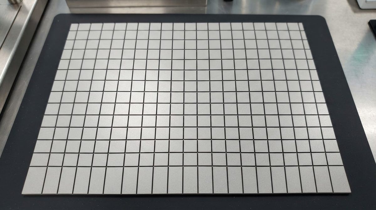
For panel singulation, AlN laser scribing is often faster and cheaper than a full through-cut. The laser scores a groove 30–50 % of the substrate thickness deep, and the panel is then snapped along the scribe line. This approach reduces laser time per part by 50–70 % and leaves a cleaner break surface on the snap side. The trade-off: edge straightness on the snapped side depends on the AlN grain structure and may show ±50–100 µm of wander. If edge straightness matters, a full through-cut or post-snap grinding is needed.
Post-Machining Surface Quality
Laser-cut edges on AlN typically measure Ra 1.0–3.0 µm. If your design requires a smoother edge—for instance, to reduce particle generation in cleanroom environments—lapping or polishing is the next step. AlN surface roughness specifications are worth reviewing before finalising your drawing, because specifying Ra < 0.4 µm on a laser-cut edge adds a secondary operation and cost.
When Not to Use Aluminum Nitride AlN Laser Machining
Laser machining is not always the right call. Consider alternatives in these situations:
- Very thick substrates (> 1.5 mm): Diamond-blade dicing or diamond wire sawing may be more practical, despite higher tool wear, because laser cut time and taper become excessive.
- Extremely tight edge tolerances (< ±10 µm): Grinding or lapping after laser cutting is needed. The laser alone cannot hold single-digit-micron tolerances consistently.
- High-volume simple shapes: If the geometry is a plain rectangle with no internal features, green-machining (shaping before sintering) can be cheaper at volumes above 10,000 pieces.
- Budget-driven projects where alumina would suffice: If the thermal load does not demand AlN’s 170–200 W/mK conductivity, 96 % alumina at roughly one-third the substrate cost is the pragmatic choice. AlN’s material cost amplifies the impact of any machining scrap.
Thickness and Tolerance Considerations
Aluminum nitride AlN laser machining parameters must be re-qualified whenever substrate thickness changes. A parameter set tuned for 0.38 mm AlN will over-cut or under-cut on 0.635 mm or 1.0 mm material. Review AlN substrate thickness and tolerance options early in the design phase so the machining vendor can lock in process parameters before prototyping.
Frequently Asked Questions
Can a standard PCB fab house laser-cut AlN?
Most FR-4 fab houses do not stock ceramic-capable laser systems. AlN requires either a CO₂ or UV laser with ceramic-specific process recipes and a vacuum chuck. Work with a ceramic substrate specialist that has validated parameters for your thickness.
Does laser cutting change AlN’s thermal conductivity?
Bulk thermal conductivity is unaffected. The HAZ—typically 20–150 µm wide—may have slightly degraded thermal properties due to micro-cracking and grain-boundary oxidation, but this zone is too narrow to measurably impact heat spreading across the substrate.
What is the smallest hole a laser can drill in AlN?
UV lasers can drill vias as small as 50 µm diameter in AlN substrates up to 0.38 mm thick. CO₂ lasers bottom out around 100–120 µm diameter due to their longer wavelength and larger focused spot size.
Is laser machining safe for metallised AlN substrates?
Yes, provided the laser path stays at least 150–200 µm from metallisation edges. Closer cuts risk thermal damage to the metal-ceramic interface, which can cause delamination. Design your cut lines with adequate clearance and communicate keep-out zones clearly on the fabrication drawing.
How does AlN laser machining compare to Si₃N₄?
Silicon nitride is tougher (fracture toughness ~6–7 MPa·m⁰·⁵ vs. AlN’s ~2.5–3.5 MPa·m⁰·⁵) but absorbs CO₂ laser energy less efficiently, requiring more passes and slower feed speeds. Si₃N₄ laser scribing details are covered separately.