Aluminum nitride (AlN) is a ceramic substrate material with thermal conductivity of 170–200 W/mK at 25 °C—roughly six to eight times higher than 96% alumina—and a coefficient of thermal expansion (CTE) of 4.4–4.7 ppm/°C, closely matched to silicon and SiC die. An aluminum nitride AlN custom PCB pairs this thermal performance with metallization processes such as DBC, DPC, or AMB to create circuit boards that handle heat fluxes impossible on FR-4 or standard metal-core PCBs.
Key Takeaways
- AlN substrates conduct heat at 170–200 W/mK (per Kyocera SH-30 and Maruwa AN-200 datasheets), compared with 24–28 W/mK for 96% alumina.
- CTE of 4.4–4.7 ppm/°C reduces solder-joint stress when bonding bare silicon (2.6 ppm/°C) or SiC (4.0 ppm/°C) die directly to the substrate.
- AlN costs three to five times more per unit area than 96% alumina, so it is justified only when the thermal budget demands it.
- Fabrication of an aluminum nitride AlN custom PCB typically uses DBC (direct bond copper), DPC (direct plated copper), or AMB (active metal brazing); HTCC and LTCC are not standard processes for AlN boards.
- Moisture sensitivity requires storage in nitrogen or vacuum-sealed packaging; AlN hydrolyzes slowly in humid air, degrading surface conductivity over time.
What Makes an Aluminum Nitride AlN Custom PCB the Right Choice for High-Power Designs
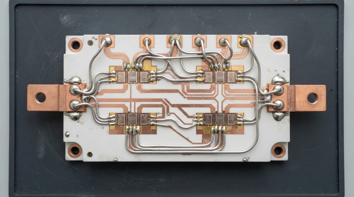
The primary reason to specify AlN over alumina or FR-4 is thermal resistance. A 0.635 mm thick AlN substrate with an area of 25 × 25 mm has a through-thickness thermal resistance of roughly 0.07 °C/W (using k = 180 W/mK). The same geometry in 96% alumina yields approximately 0.40 °C/W. That difference translates directly into lower junction temperatures or higher allowable power dissipation.
AlN’s dielectric properties also matter: a dielectric constant of 8.5–9.0 at 1 MHz and dielectric strength above 15 kV/mm (per CoorsTek ADS-996 datasheet) make it suitable for high-voltage isolation in power modules. The low dielectric loss tangent (0.0003–0.001 at 1 MHz) supports RF and microwave applications up to several GHz.
AlN Material Properties at a Glance
| Parameter | Value | Unit | Condition | Source |
|---|---|---|---|---|
| Thermal conductivity | 170–200 | W/mK | 25 °C | Kyocera SH-30 / Maruwa AN-200 |
| CTE | 4.4–4.7 | ppm/°C | 25–400 °C | Kyocera SH-30 |
| Dielectric constant (εr) | 8.5–9.0 | — | 1 MHz, 25 °C | CoorsTek ADS-996 |
| Dielectric strength | ≥ 15 | kV/mm | 25 °C | CoorsTek ADS-996 |
| Flexural strength | 300–400 | MPa | 3-point bend, ASTM C1161 | Maruwa AN-200 |
| Density | 3.26–3.30 | g/cm³ | — | Kyocera SH-30 |
| Max continuous use temp. | 1 000 | °C | In inert atmosphere | CeramTec Alunit |
Typical values for commercially available material, for comparison only. Confirm against the datasheet for your specific grade.
Fabrication Processes for an Aluminum Nitride AlN Custom PCB
Three metallization processes dominate aluminum nitride AlN custom PCB production. Each suits a different combination of copper thickness, line resolution, and thermal cycling requirement.
DBC (Direct Bond Copper)
DBC bonds a copper foil (typically 0.127–0.30 mm) to the AlN surface through a controlled-atmosphere oxidation process at approximately 1 065 °C. The result is a high-adhesion copper layer capable of carrying hundreds of amps. DBC is the standard for IGBT and SiC power modules where copper thickness above 0.20 mm is required. Minimum trace/space is typically 0.30–0.50 mm, limiting circuit density.
DPC (Direct Plated Copper)
DPC uses sputtered seed layers and electroplated copper, achieving copper thickness of 1–100 µm with minimum trace/space down to 50 µm or finer. This process suits applications such as UV LED arrays and high-frequency RF circuits where fine features and tight tolerances matter more than bulk current capacity.
AMB (Active Metal Brazing)
AMB uses a titanium-containing braze alloy (such as Ag-Cu-Ti) to bond copper foil to the AlN at roughly 800–900 °C. AMB joints survive thermal cycling better than DBC joints, making this the preferred process for automotive-grade SiC power modules that must pass 3 000+ cycles between −40 °C and +150 °C per AQG 324. Copper thickness ranges from 0.20 mm to 0.80 mm.
For details on laser machining of AlN substrates—scribing, drilling, and via formation—a separate guide covers kerf width, heat-affected zone, and parameter selection.
Worked Example: Thermal Resistance Through an AlN DBC Substrate
Assume a 30 × 30 mm AlN DBC substrate, 0.635 mm thick, carrying a 200 W SiC MOSFET die. This example shows why engineers specify an aluminum nitride AlN custom PCB for power-dense layouts.
Through-substrate thermal resistance:
Rth = t / (k × A) = 0.000635 m / (180 W/mK × 0.0009 m²) = 0.0039 °C/W
Temperature rise through the ceramic alone:
ΔT = 200 W × 0.0039 °C/W = 0.78 °C
For comparison, the same geometry in 96% alumina (k = 26 W/mK) yields ΔT = 5.4 °C. The difference grows with thicker substrates or higher power densities, which is exactly why AlN is specified for power modules above roughly 50 W/cm².
Enter your substrate dimensions, material, and dissipated power below to estimate junction temperature rise for your own design.
Design Rules and Practical Considerations
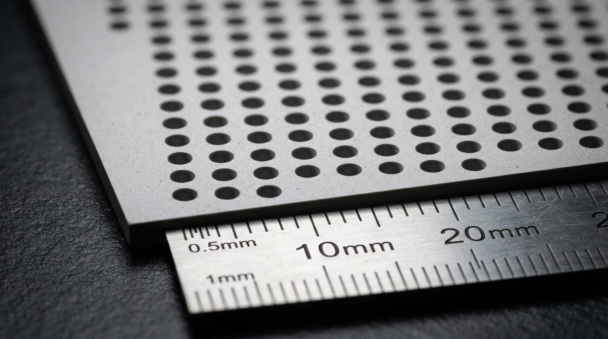
AlN is harder to process than alumina. Keep these constraints in mind during layout of any aluminum nitride AlN custom PCB.
- Moisture sensitivity. AlN reacts with water vapor to form aluminum hydroxide, which degrades surface roughness and metallization adhesion. Store bare substrates in nitrogen-purged containers. Bake at 150 °C for 2 hours before metallization if exposure has occurred.
- Mechanical handling. Flexural strength of 300–400 MPa (per ASTM C1161) is lower than Si₃N₄ (600–900 MPa). Design for uniform clamping pressure and avoid point loads during assembly. Consult the AlN mechanical strength guide for reliability data.
- Via formation. Laser drilling with CO₂ or UV lasers is standard. Minimum via diameter is typically 0.10–0.15 mm depending on substrate thickness. Filled vias using tungsten or copper paste add cost but enable double-sided circuits.
- Soldering. AlN’s CTE (4.5 ppm/°C) is far from that of copper leadframes (17 ppm/°C). Use compliant solders (e.g., SAC305 or indium-based alloys) or sintered silver for die attach to manage CTE mismatch stress.
When Not to Use AlN
AlN is expensive and hard to justify when a cheaper substrate does the job. Choose something else in these situations:
- Power density below ~10 W/cm². 96% alumina (24–28 W/mK) or an aluminum MCPCB (1–3 W/mK board-level) is adequate and costs far less.
- Large panel sizes. AlN substrates are typically limited to about 114 × 114 mm or 138 × 190 mm depending on supplier. If your design exceeds these dimensions, consider tiling or switching to alumina.
- Extreme mechanical shock. Silicon nitride (Si₃N₄) substrates offer roughly double the fracture toughness (6–7 MPa·√m vs. 2.5–3.5 MPa·√m for AlN) and are better suited for automotive underhood or aerospace vibration environments.
- Cost-sensitive consumer products. FR-4 at $0.01–0.03/cm² vs. AlN at $1–5/cm² makes the choice obvious when thermal loads are manageable.
Frequently Asked Questions
Can you solder components directly to an AlN PCB?
Yes, standard reflow soldering with SAC305 paste works on metallized AlN substrates. The metallization layer (typically Ni/Au or Ni/Pd/Au over copper) provides a solderable surface. Peak reflow temperatures of 245–260 °C are well within AlN’s capability.
How does AlN compare to BeO for thermal conductivity?
Beryllium oxide (BeO) reaches 250–300 W/mK, roughly 30–60% higher than AlN. However, BeO dust is a confirmed human carcinogen that causes chronic beryllium disease, and its use is heavily restricted in the EU and elsewhere. AlN is the standard replacement in nearly all new designs. See the AlN PCB properties and sourcing overview for a full comparison.
What surface finishes are available on AlN PCBs?
Common finishes include ENIG (electroless nickel/immersion gold), ENEPIG, and electrolytic Ni/Au. For wire-bonding pads, electrolytic gold at 0.5–1.5 µm thickness is typical. The finish choice depends on the assembly method—soldering, wire bonding, or sintered silver die attach.
Is AlN compatible with wire bonding?
Yes. Both gold and aluminum wedge bonding work on properly metallized AlN. Gold wire bonding requires a minimum gold thickness of 0.5 µm over nickel. Aluminum wedge bonding is common on thick-film metallized AlN in power module applications.
What is the typical lead time for an aluminum nitride AlN custom PCB?
Prototype quantities (1–25 pieces) typically ship in 2–4 weeks depending on metallization process and complexity. Production runs may take 4–8 weeks. Substrate availability from the ceramic blank supplier is often the longest lead-time item.
Next Step
If your thermal analysis points to AlN, the next step is matching your layout to a fabrication process—DBC for high current, DPC for fine features, AMB for extreme thermal cycling. Upload your design files for a quote and process recommendation.