Aluminum nitride (AlN) ceramic PCBs tolerate continuous operating temperatures above 300 °C, conduct heat at 170–230 W/mK, and maintain stable dielectric performance under vibration, altitude, and rapid thermal cycling. For any aerospace defense PCB application, an AlN PCB delivers the exact combination of thermal, electrical, and mechanical performance that sealed military enclosures demand. Where FR-4 degrades above 130 °C and standard alumina hits thermal limits in high-flux designs, AlN gives system designers a substrate that keeps power devices, radar modules, and EW assemblies running with minimal or no forced airflow.
Why Aerospace Defense PCB Programs Specify AlN PCB Substrates
Avionics bays, missile seekers, satellite power converters, and electronic warfare pods share a common constraint: heat must leave the device through conduction alone, often into a cold plate or chassis, with no fan and sometimes no convection at all. AlN’s thermal conductivity of 170–230 W/mK (per Kyocera SH-30 and Maruwa AN-230 datasheets, measured at 25 °C per ASTM E1461) is six to eight times higher than 96% alumina (24–28 W/mK). That difference translates directly into lower junction temperatures for GaN HEMTs, SiC MOSFETs, and high-power laser diodes mounted on the substrate.
Beyond thermal performance, AlN offers a coefficient of thermal expansion (CTE) of 4.4–4.7 ppm/°C at 25–400 °C. This closely matches silicon (2.6 ppm/°C), SiC (4.0 ppm/°C), and GaN-on-SiC (≈4.2 ppm/°C). A tight CTE match between substrate and die is critical in defense applications that see –55 °C to +200 °C thermal cycling per MIL-STD-883, Method 1010. Mismatched CTE causes solder joint fatigue and die cracking — failure modes that are not repairable in orbit or on a missile.
Key Material Properties for Defense-Grade AlN PCB Substrates
| Parameter | AlN (typical) | Unit | Condition | Source |
|---|---|---|---|---|
| Thermal conductivity | 170–230 | W/mK | 25 °C, ASTM E1461 | Kyocera SH-30 / Maruwa AN-230 |
| Dielectric constant (εr) | 8.5–8.9 | — | 1 MHz, 25 °C | CoorsTek AlN datasheet |
| Dielectric strength | 14–17 | kV/mm | 25 °C, IEC 60672 | Kyocera SH-30 |
| CTE | 4.4–4.7 | ppm/°C | 25–400 °C | Maruwa AN-230 |
| Flexural strength | 300–400 | MPa | ASTM C1161, 3-pt bend | CoorsTek / Kyocera |
| Volume resistivity | >1014 | Ω·cm | 25 °C | CoorsTek AlN |
| Max continuous use temp. | 1000 (inert atm.); ~800 (in air) | °C | Oxidation-limited in air | Kyocera technical note |
Typical values for commercially available material, for comparison only. Confirm against the datasheet for your specific grade.
One detail engineers sometimes overlook: AlN oxidizes in air above roughly 700–800 °C, forming an alumina surface layer that degrades thermal performance over time. In sealed or inert-atmosphere enclosures common in space hardware, this is not a concern. For air-breathing platforms, 300–400 °C continuous operation is routine and well within safe margins.
Common Aerospace Defense PCB and AlN PCB Use Cases
The following applications represent the most frequent reasons defense programs select an AlN PCB over alumina or organic alternatives:
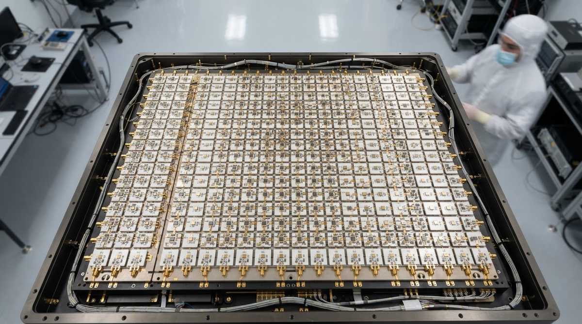
- Radar T/R modules: GaN-on-SiC MMICs in active electronically scanned arrays (AESA) dissipate 5–15 W per element in pulsed operation. AlN substrates under each MMIC reduce thermal resistance from die to cold plate, keeping junction temperatures within the GaN device’s rated limit (typically 225 °C channel temperature per Wolfspeed/Cree CGH-series datasheets).
- Satellite power electronics: DC-DC converters and battery charge regulators on spacecraft rely on conduction cooling through the chassis. AlN DBC (direct bond copper) substrates carry high current while conducting waste heat efficiently into the satellite’s thermal bus.
- EW and jamming systems: High-duty-cycle RF amplifiers in electronic warfare pods generate sustained heat loads. AlN’s combination of high thermal conductivity and low dielectric loss tangent (0.001–0.003 at 1 MHz) makes it suitable for substrates directly under the RF signal path.
- Laser designators and directed energy: High-power laser diode arrays mounted on AlN submounts benefit from the same thermal path advantages used in commercial laser and photonics assemblies, but with the added requirement of surviving shock loads up to 40 g per MIL-STD-810.
Similar thermal demands exist in SiC power module substrates used in defense power converters, where the aerospace defense PCB must handle both high current and rapid thermal transients.
Worked Example: Thermal Resistance Through an AlN PCB Substrate
Consider a GaN HEMT die dissipating 10 W mounted on an AlN substrate. The substrate is 0.635 mm thick, and the heat spreads across a footprint of 10 mm × 10 mm (100 mm²).
One-dimensional thermal resistance through the substrate:
Rth = t / (k × A)
Rth = 0.000635 m / (200 W/mK × 0.0001 m²) = 0.032 °C/W
Temperature rise through the substrate alone: ΔT = 10 W × 0.032 °C/W = 0.32 °C.
For comparison, the same geometry in 96% alumina (k = 25 W/mK) yields Rth = 0.254 °C/W and ΔT = 2.54 °C. The AlN PCB contributes roughly eight times less thermal resistance. In a real stack with solder layers, TIM, and cold plate interface, that 2.2 °C savings at the substrate level can be the margin between meeting and exceeding the device’s rated junction temperature.
Enter your substrate area, thickness, and dissipated power below to estimate junction temperature rise for your own aerospace defense PCB design.
Metallization and Assembly Considerations for AlN PCB
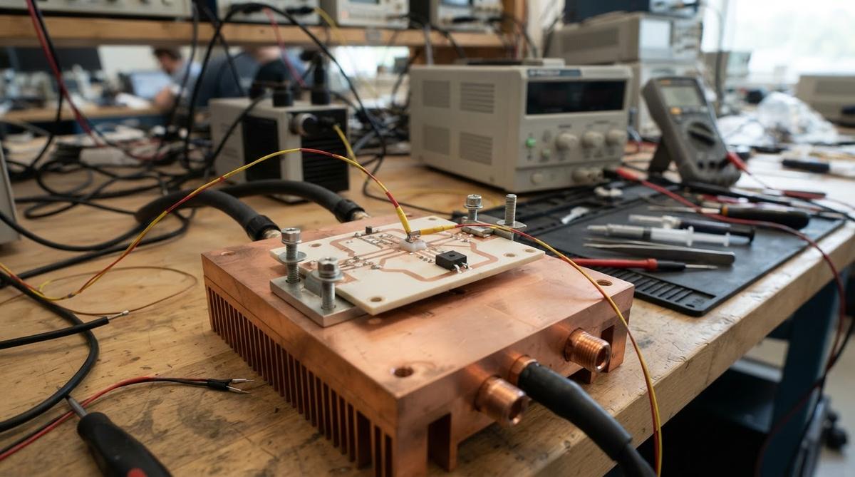
AlN substrates for defense programs are typically metallized using DBC (direct bond copper), AMB (active metal brazing), or thin-film sputtered Ti/Pt/Au or TiW/Ni/Au stacks. DBC offers thick copper (0.15–0.50 mm) for high current, while thin-film metallization enables fine-line patterning (trace/space down to 25–50 µm) for RF circuits.
One practical issue: AlN’s surface reacts with moisture, forming aluminum hydroxide, which weakens adhesion. Substrates should be stored in dry nitrogen and metallized promptly after lapping. For long-shelf-life defense inventory, hermetic packaging or conformal coating protects exposed AlN surfaces.
For programs requiring custom AlN fabrication with specific metallization stacks, lead times are typically longer than alumina due to the controlled-atmosphere sintering AlN requires.
When NOT to Use an AlN PCB in Aerospace and Defense
Cost-sensitive, moderate-thermal designs. AlN substrates cost three to five times more per unit area than 96% alumina. If your device dissipates under 1–2 W and operates below 200 °C, alumina or even metal-core PCBs may be adequate.
Large panel sizes. AlN substrates are typically available up to about 114 mm × 114 mm (some suppliers offer 140 mm × 190 mm). For large-area boards, alumina or Si₃N₄ may be more practical.
Mechanical shock without proper support. AlN is stiffer but more brittle than Si₃N₄ (fracture toughness ~2.5 MPa·m0.5 vs. 5–7 MPa·m0.5 for Si₃N₄). In applications with severe mechanical shock and no potting or structural support, Si₃N₄ may be the better ceramic.
Low-frequency, non-thermal applications. If your board has no significant heat load and operates at frequencies where FR-4’s dielectric loss is acceptable, there is no reason to pay for a ceramic aerospace defense PCB.
Frequently Asked Questions
Does AlN meet MIL-spec outgassing requirements for space?
AlN ceramic itself easily passes NASA ASTM E595 outgassing requirements (TML < 1.0%, CVCM < 0.1%) because it is a fully sintered inorganic material with no volatile content. Outgassing risk comes from solder paste flux residues, adhesives, or conformal coatings applied during assembly, not from the substrate.
Can AlN substrates handle the thermal shock of a missile launch?
AlN has a thermal shock resistance parameter (R = σf/Eα) that tolerates rapid temperature swings of several hundred degrees Celsius. Substrates routinely pass MIL-STD-883 Method 1011 thermal shock testing (–65 °C to +150 °C, 15 cycles minimum). Thinner substrates (0.25–0.38 mm) perform better under thermal shock than thicker ones because the through-thickness temperature gradient is smaller.
Is AlN approved for use in ITAR-controlled programs?
AlN ceramic itself is not export-controlled under ITAR or EAR as a raw material. The controlled items are the assemblies, designs, and end-use applications. Sourcing AlN substrates from qualified suppliers with appropriate documentation (C of C, material traceability) satisfies most defense prime contractor procurement requirements.
How does AlN compare to BeO for defense thermal substrates?
Beryllium oxide (BeO) offers slightly higher thermal conductivity (250–300 W/mK) than AlN, but BeO dust is a confirmed human carcinogen that causes chronic beryllium disease. Handling, machining, and disposal of BeO require stringent OSHA controls. Most new defense programs have moved to AlN to avoid the health, safety, and lifecycle cost burden of BeO. For more information on beryllia hazards, see OSHA’s beryllium standards (29 CFR 1910.1024).
What surface finishes work on AlN for wire bonding?
Thin-film Ti/Pt/Au or TiW/Ni/Au metallization on AlN supports both gold and aluminum wire bonding. Gold wire bonding to a plated Au surface is standard for defense hybrids. Aluminum wedge bonding requires a clean, oxide-free Au or Al pad surface. Finish selection depends on the bonding wire and the assembly house’s qualified process.
Next Step
If your program requires AlN substrates with specific metallization, thickness, or panel size, review the available options for AlN thin substrates or request a quotation with your mechanical drawing and material callout. Engineering support is available to review your thermal stack and recommend a substrate grade.