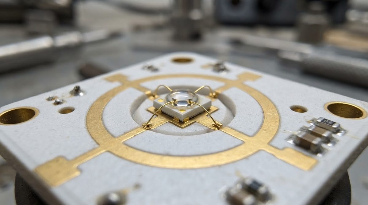
When engineers design a UV LED PCB, an AlN PCB is the default substrate choice—and for good reason. Aluminum nitride conducts heat at 170–200 W/mK (roughly 7× better than 96% alumina), does not degrade under prolonged deep-UV exposure below 280 nm, and closely matches the CTE of GaN-on-sapphire die. FR-4 and metal-core PCBs yellow, crack, or outgas under UV-C flux within hundreds of hours. AlN does not.
Why a UV LED PCB Demands an AlN PCB Substrate
UV-C LEDs (200–280 nm) used in water disinfection, surface sterilization, and analytical instruments present a harsh combination of demands. The GaN-based die run hot—wall-plug efficiency for commercial UV-C LEDs is still only 3–10% (per Nichia and Seoul Viosys published specs), meaning 90–97% of input power converts directly to heat. At the same time, the short-wavelength photons attack organic materials. Silicone encapsulants degrade. FR-4 resin darkens and delaminates. Even standard white solder mask absorbs UV-C and breaks down within weeks of continuous operation.
AlN is fully inorganic. It has no resin, no organic binder in its fired state, and no polymer layer to degrade. Its optical reflectance in the UV-C band is low (it absorbs rather than reflects), but that absorption does not cause chemical breakdown. The substrate stays mechanically and thermally stable for the full rated life of the LED die—typically 10,000 to 30,000 hours at L70. This is why every serious UV LED PCB design at UV-C wavelengths specifies an AlN PCB as the foundation.
The thermal path matters just as much. A UV-C LED die dissipating 2 W across a 1 mm × 1 mm footprint produces a heat flux of 200 W/cm². Without a high-conductivity substrate directly beneath the die, junction temperature rises fast. Every 10 °C increase in junction temperature roughly halves the useful life of a UV-C LED, per data published by Seoul Viosys and Crystal IS (an Asahi Kasei company).
Thermal Comparison: AlN vs. Alumina vs. MCPCB for UV LEDs
| Parameter | AlN | Al₂O₃ 96% | Aluminum MCPCB | Unit | Condition |
|---|---|---|---|---|---|
| Thermal conductivity | 170–200 | 24–28 | 1–4 (dielectric layer) | W/mK | 20 °C, bulk |
| CTE | 4.4–4.7 | 6.5–7.2 | 22–24 (Al base) | ppm/°C | 20–300 °C |
| UV-C stability (280 nm, 5 000 h) | No degradation | No degradation | Resin darkens, delaminates | — | Continuous exposure |
| Dielectric strength | 14–17 | 10–15 | 3–6 (dielectric layer) | kV/mm | ASTM D149 |
| Max continuous use temp. | 1 000+ | 1 000+ | 130–150 (resin limited) | °C | In air |
Typical values for commercially available material, for comparison only. Confirm against the datasheet for your specific grade.
The dielectric layer in a metal-core PCB (MCPCB) is the bottleneck. Even “high-performance” MCPCB dielectrics top out around 4 W/mK. For a UV-C LED pushing 200 W/cm², that layer creates a thermal resistance roughly 50× higher than the same thickness of AlN. Alumina is UV-stable but its 24–28 W/mK conductivity limits it to lower-power UV-A (365–395 nm) applications where heat flux is more manageable.
CTE Match to GaN-on-Sapphire Die
Most UV and UV-C LED die are GaN grown on sapphire substrates. Sapphire has a CTE of approximately 5.0–7.7 ppm/°C (depending on crystal axis and temperature range, per Kyocera sapphire datasheets). AlN at 4.4–4.7 ppm/°C is a closer match than aluminum MCPCB at 22–24 ppm/°C. This matters because the die is often bonded with AuSn solder or sintered silver, both of which form rigid joints. A large CTE mismatch across hundreds of thermal cycles fractures the bond line or cracks the die.
For UV-C LEDs in sterilization systems that cycle on and off thousands of times per year, this CTE match directly extends field life. It is one of the key reasons an AlN PCB outperforms every organic-based alternative in UV LED PCB reliability testing.
Worked Example: Junction Temperature on AlN vs. 96% Alumina
Assume a UV-C LED die dissipating 1.5 W through a 1 mm × 1 mm contact area on a 0.635 mm thick substrate, with a perfect thermal interface on both sides.
Thermal resistance through the substrate (Rth = t / (k × A)):
- AlN (k = 180 W/mK): Rth = 0.000635 / (180 × 0.000001) = 3.53 °C/W
- Al₂O₃ 96% (k = 26 W/mK): Rth = 0.000635 / (26 × 0.000001) = 24.4 °C/W
Temperature rise (ΔT = P × Rth):
- AlN: 1.5 W × 3.53 °C/W = 5.3 °C
- Al₂O₃ 96%: 1.5 W × 24.4 °C/W = 36.6 °C
That 31 °C difference through the substrate alone can be the difference between a junction temperature of 85 °C (within safe operating range) and 116 °C (accelerated degradation). This calculation ignores spreading resistance, solder joint resistance, and heat-sink interface resistance—all of which add to the total—so the real-world gap is even more consequential at higher power levels.
Enter your own substrate area, thickness, and dissipated power below to estimate junction temperature rise for your UV LED PCB or AlN PCB design.
Substrate Selection: Surface Finish and Thickness
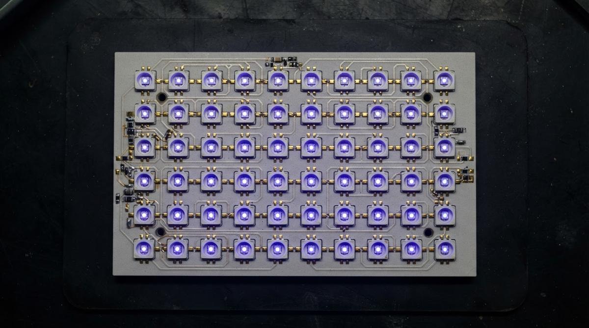
UV LED packaging typically uses polished or lapped AlN substrates when die are bonded with eutectic solder, because surface roughness directly affects void fraction in the bond line. A surface roughness (Ra) below 0.1 µm is common for AuSn die attach. For wire-bonded designs where metallization is applied by thin-film sputtering, a polished surface also improves adhesion and trace definition.
Thinner substrates—0.25 mm or 0.38 mm—reduce total thermal resistance but are more fragile during handling and reflow. For single-die UV-C modules, thin AlN substrates in the 0.25–0.50 mm range are standard. Multi-die arrays on larger panels may use 0.635 mm for mechanical stability.
When circuit patterns are needed (traces, pads, thermal vias), custom AlN PCB fabrication with DPC (direct plated copper) or thin-film metallization provides line/space resolution suitable for UV LED driver integration on the same substrate.
When Not to Use AlN for UV LEDs
An AlN PCB costs 3–5× more per unit area than 96% alumina. If your application is UV-A (365–395 nm) at moderate power (under 1 W per die), alumina or even custom 96% alumina substrates may be sufficient. UV-A photons are less damaging to organics, and the lower heat flux relaxes the thermal requirement. Not every UV LED PCB needs aluminum nitride.
For prototyping or low-volume UV-C work where cost is the primary constraint and lifetime requirements are short (under 1,000 hours), alumina with proper metallization can serve as a development platform, with the understanding that thermal performance will limit maximum drive current.
If your design is a large-area panel (greater than 100 mm × 100 mm) with many low-power UV LEDs, an MCPCB with UV-resistant white solder mask may work—but verify mask stability at your specific wavelength and irradiance. Most standard masks fail below 300 nm.
FAQ
Does AlN absorb UV-C light?
Yes, AlN absorbs in the UV-C range rather than reflecting it. However, this absorption does not cause chemical degradation or mechanical weakening. The substrate remains stable for the full rated life of the LED. If you need a reflective substrate surface, a reflective metal coating (such as aluminum thin film) can be applied over the AlN.
Can I solder UV-C LED die directly to an AlN substrate?
Yes. AlN substrates are commonly metallized with Ti/Pt/Au or Ti/Ni/Au thin-film stacks, then bonded with AuSn eutectic solder (80Au/20Sn, melting at 280 °C) or sintered silver paste. The metallization must be applied to a clean, polished surface for reliable wetting.
How does AlN compare to silicon nitride for UV LED packaging?
Silicon nitride (Si₃N₄) offers superior mechanical toughness (fracture toughness ~6–7 MPa·m¹/² vs. ~2.5–3.5 for AlN) but lower thermal conductivity (typically 70–90 W/mK for commercial grades). For UV LED PCB applications where thermal performance is the priority and mechanical shock is not severe, an AlN PCB is the better choice. Si₃N₄ is more common in power modules subject to thermal cycling stress. See custom Si₃N₄ substrates for details on that material.
What metallization works on AlN for UV LED substrates?
Thin-film sputtered metallization (Ti/Pt/Au or Ti/Cu/Ni/Au) is standard for UV LED die attach pads. DPC (direct plated copper) is used when thicker copper traces are needed for driver circuitry. Thick-film printing with tungsten or molybdenum pastes is possible but less common for UV LED packaging because surface finish is coarser.
What is the typical substrate size for a UV-C LED module?
Single-emitter UV-C modules commonly use AlN substrates between 3 mm × 3 mm and 10 mm × 10 mm, with thickness from 0.25 mm to 0.635 mm. Multi-emitter arrays for water treatment reactors may use substrates up to 25 mm × 50 mm or larger, depending on the optical and thermal layout.
Next Step
If you are specifying an AlN PCB for a UV or UV-C LED package, start by defining your die attach method, required surface finish, and substrate dimensions. For laser-scribed AlN substrates with snap-apart arrays, or custom metallized AlN boards, request a quote with your drawing and we will confirm feasibility and lead time.