Aluminum nitride (AlN) is a polycrystalline ceramic with thermal conductivity in the 170–230 W/mK range (grade-dependent, measured at 25 °C per ASTM E1461), a close CTE match to silicon (4.5–4.6 ppm/°C vs. Si at 2.6 ppm/°C), and volume resistivity above 10¹² Ω·cm. These properties make it the substrate of choice for high-power electronics where heat must leave the die fast and the thermal path must stay electrically insulating. Choosing the right aluminum nitride AlN manufacturer means verifying material grade, metallization capability, and dimensional tolerances—not just price per piece.
Key Takeaways
- Commercial AlN substrates range from 170 W/mK (standard grade) to 230 W/mK (high-purity grade), per Maruwa and Kyocera published datasheets.
- AlN is compatible with DBC, AMB, thin-film (sputtered), and thick-film metallization—but not with HTCC or LTCC co-firing processes used for alumina multilayers.
- CTE mismatch between AlN (4.5 ppm/°C) and copper (17 ppm/°C) drives warpage risk; substrate thickness and copper thickness must be balanced during design.
- AlN costs 3–5× more per unit area than 96% Al₂O₃, so it is justified only when thermal resistance savings translate into real system-level gains.
- Surface finish and flatness matter: lapped AlN can reach Ra ≤ 0.05 µm, critical for solder or sinter die-attach yield.
What Makes AlN Different from Other Ceramic Substrates
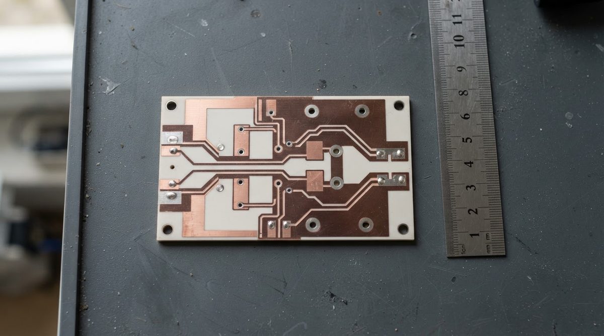
Alumina (Al₂O₃ 96%) dominates ceramic PCB volumes because it is cheap, well-characterized, and available everywhere. Its thermal conductivity sits at 24–28 W/mK (25 °C, per CoorsTek ADS-996 datasheet). For many LED, sensor, and RF circuits, that is sufficient. AlN enters the picture when the power density exceeds what alumina can handle without excessive junction temperature rise.
Silicon nitride (Si₃N₄) offers superior fracture toughness (6–7 MPa·m¹/², per Kyocera SN-220 datasheet) and is increasingly used in EV power modules. But its thermal conductivity tops out around 80–90 W/mK—less than half of AlN. If raw thermal performance is the primary driver and mechanical shock is manageable, AlN wins. If the substrate must survive severe thermal cycling without cracking, Si₃N₄ ceramic PCBs deserve a closer look.
AlN Material Grades and Properties
| Parameter | Standard AlN | High-Purity AlN | Unit | Condition | Source |
|---|---|---|---|---|---|
| Thermal conductivity | 170–180 | 200–230 | W/mK | 25 °C, ASTM E1461 | Maruwa AN-200 / AN-230 datasheets |
| Dielectric constant (εr) | 8.5–8.9 | 8.6–8.9 | — | 1 MHz, 25 °C | Kyocera SH-30 datasheet |
| Dielectric strength | 15–17 | 15–17 | kV/mm | 25 °C | CoorsTek |
| CTE | 4.5 | 4.6 | ppm/°C | 25–400 °C | Maruwa |
| Flexural strength | 300–350 | 300–400 | MPa | 3-pt bend, ASTM C1161 | Kyocera |
| Volume resistivity | >10¹⁴ | >10¹⁴ | Ω·cm | 25 °C | Maruwa |
Typical values for commercially available material, for comparison only. Confirm against the datasheet for your specific grade.
The gap between 170 and 230 W/mK is real and measurable at the system level. For a 10 × 10 mm die dissipating 100 W through a 0.635 mm thick substrate, the conductive thermal resistance (Rth = t / (k × A)) drops from 0.037 °C/W at 170 W/mK to 0.028 °C/W at 230 W/mK. That 0.009 °C/W difference means roughly 0.9 °C lower junction temperature at 100 W—modest alone, but it compounds with interface and heatsink resistances in a real stack. High-purity AlN is worth specifying when every fraction of a degree counts, such as in aerospace and defense power assemblies or GaN RF amplifiers.
Metallization Processes for AlN PCBs
Raw AlN is just a substrate. The metallization process defines what you can do with it electrically and thermally. Each process suits a different power level and circuit complexity.
DBC (Direct Bonded Copper)
DBC bonds a copper foil (typically 0.127–0.3 mm) to AlN using a controlled Cu₂O eutectic oxidation layer at roughly 1065 °C. It produces thick copper traces capable of carrying hundreds of amps and spreading heat laterally. AlN DBC substrates are the default for IGBT and SiC MOSFET power modules. The trade-off: trace resolution is limited to about 0.15–0.2 mm line/space after etching, and the high-temperature bonding cycle can introduce residual stress.
AMB (Active Metal Brazing)
AMB uses an AgCuTi braze alloy to bond copper at around 780–850 °C. The active titanium wets the AlN surface directly, producing a stronger bond than DBC—peel strength typically 8–12 N/mm versus 4–6 N/mm for DBC (per Rogers curamik technical notes). AMB allows thicker copper (up to 0.8 mm) and survives more aggressive thermal cycling. AlN AMB substrates are gaining traction in SiC traction inverters for EVs.
Thin Film and Thick Film
For RF, sensor, and high-density interconnect applications, sputtered thin-film metallization (TiW/Au, NiCr/Au, or Ti/Pt/Au) achieves line/space down to 10–25 µm on polished AlN. AlN thin-film substrates are common in mmWave modules and laser diode carriers. Thick-film AlN substrates use screen-printed tungsten or gold conductors and are suited for heater circuits, resistor networks, and hybrid modules where trace width below 100 µm is not required.
Worked Example: Thermal Resistance Comparison
Suppose you are mounting a SiC die (5 × 5 mm) on a 25.4 × 25.4 mm substrate, 0.635 mm thick, with a 0.3 mm DBC copper layer on each side. Compare AlN vs. 96% alumina:
Ceramic conductive resistance only (Rth = t / (k × A)):
| Substrate | k (W/mK) | t (mm) | A (mm²) | Rth,ceramic (°C/W) |
|---|---|---|---|---|
| 96% Al₂O₃ | 26 | 0.635 | 645 | 0.038 |
| AlN (standard) | 170 | 0.635 | 645 | 0.0058 |
| AlN (high-purity) | 230 | 0.635 | 645 | 0.0043 |
At 200 W dissipation, the alumina substrate alone contributes 7.6 °C of temperature rise. Standard AlN drops that to 1.2 °C. In a system where the total junction-to-ambient budget is 40 °C, saving 6.4 °C in the substrate frees margin for a smaller heatsink or higher power density.
What to Verify When Choosing an AlN Manufacturer
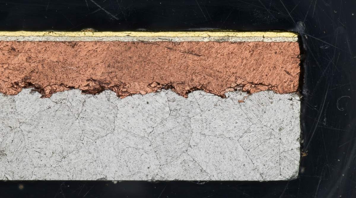
Not all AlN suppliers control the full chain from raw substrate to metallized, tested board. Here is what to check before committing a design:
- Substrate source and grade. Ask for the raw substrate manufacturer and datasheet. Thermal conductivity varies 30% between grades.
- Metallization in-house or outsourced. If DBC or AMB is outsourced, your lead time and quality control depend on two companies, not one.
- Surface finish and flatness. For die-attach, request Ra and TTV (total thickness variation) specs. A polished or lapped AlN surface with Ra ≤ 0.1 µm is typical for sinter attach.
- Dimensional tolerances. Laser-scribed AlN can hold ±0.05 mm on outline dimensions; verify this against your housing fit.
- Testing. Confirm whether hipot, visual inspection, and dimensional measurement are performed on every unit or on a sampling basis.
A structured evaluation process matters here. A guide on evaluating ceramic PCB manufacturers covers the broader checklist.
When Not to Use AlN
AlN is not the default. It is the exception you reach for when the thermal math demands it.
- Power density below ~5 W/cm²: 96% alumina or even metal-core PCBs handle this range at a fraction of the cost.
- Severe mechanical shock or vibration: AlN fracture toughness is 2.5–3.5 MPa·m¹/². Si₃N₄ at 6–7 MPa·m¹/² is far more forgiving for automotive or defense environments with repeated thermal cycling.
- Large panel sizes (>150 × 150 mm): AlN substrates are sintered at ~1800 °C in nitrogen. Large blanks are expensive and prone to warpage. Alumina is available in much larger panels.
- Cost-sensitive consumer electronics: At 3–5× the price of alumina, AlN is hard to justify for products shipping millions of units unless thermal failure rates prove it necessary.
- Multilayer circuits (>2 metal layers): AlN is not processed via HTCC or LTCC. If you need embedded vias and three or more conductor layers, alumina-based HTCC or LTCC is the practical choice.
Frequently Asked Questions
Can AlN substrates be soldered with standard lead-free solder?
Yes, once the AlN surface is metallized (typically with Ni/Au or Ag finish over the base metallization), standard SAC305 or AuSn solder reflow applies. Bare AlN cannot be wetted by solder. The metallization stack and its adhesion are what determine solder joint reliability.
Does AlN degrade in humid environments?
Unprotected AlN reacts slowly with moisture to form aluminum hydroxide, which can roughen the surface over months. Metallization and passivation layers prevent this in practice. For long-term outdoor or high-humidity exposure, confirm the manufacturer applies a hermetic or conformal coating strategy.
What is the maximum operating temperature for an AlN PCB?
The ceramic itself is stable above 1000 °C. The practical limit is set by the metallization: DBC copper oxidizes above roughly 400 °C in air, and solder joints fail well below that. Most AlN power modules are rated for continuous operation at 150–300 °C depending on the interconnect materials.
How does AlN compare to BeO on thermal conductivity?
Beryllium oxide reaches 250–300 W/mK, higher than most AlN grades. However, BeO dust is a confirmed human carcinogen and causes chronic beryllium disease. Regulatory restrictions (OSHA PEL: 0.2 µg/m³) and disposal costs make BeO impractical for new designs in most industries. High-purity AlN at 200–230 W/mK closes much of the gap without the toxicity burden.
What minimum order quantities are typical for AlN substrates?
Prototype runs of 5–25 pieces are common. Production MOQs vary by manufacturer and substrate size but often start at 50–100 pieces for standard dimensions. Custom sizes or non-standard metallization may require higher minimums due to setup costs.
Next Step
If your thermal stack-up points toward AlN, start by defining the substrate grade, metallization process, and surface finish your design requires. For custom AlN PCB fabrication, upload your Gerber files or substrate drawing to get a specification review and quote.