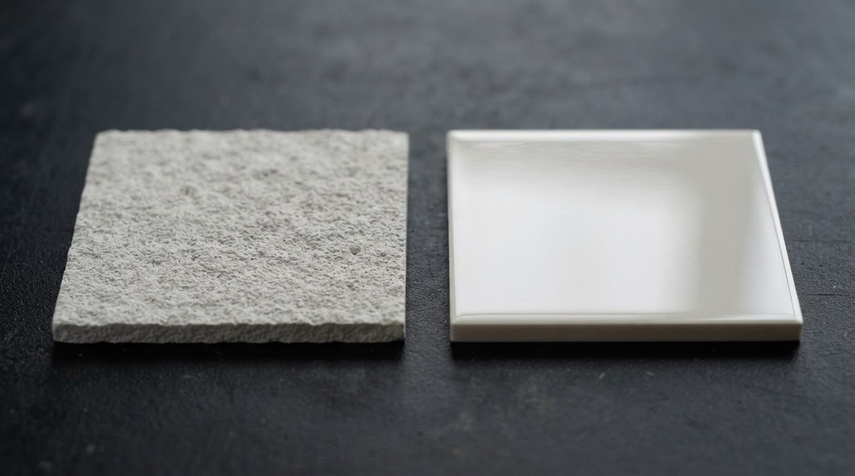
Aluminum nitride AlN polished substrates achieve surface roughness values of Ra ≤0.05 µm (50 nm), compared with Ra 0.3–0.8 µm for as-fired AlN. That difference matters for two reasons: thin-film metallization adhesion and solder-void percentage during die attach. If your process requires sputtered or evaporated metal layers thinner than 1 µm, or if your thermal interface demands void coverage below 5%, an aluminum nitride AlN polished substrate is the practical starting point.
What “Polished” and “Lapped” Mean for Aluminum Nitride AlN Polished Substrates
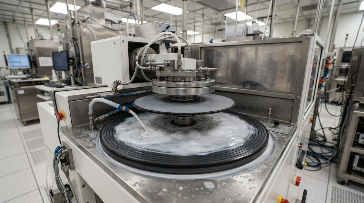
The terms are sometimes used interchangeably, but they describe different finishing steps. Lapping uses a fixed-abrasive or loose-abrasive plate to flatten the substrate and reduce roughness to roughly Ra 0.1–0.25 µm. Polishing follows lapping with a finer abrasive slurry (often colloidal silica) on a soft pad, pushing roughness below Ra 0.05 µm. Some suppliers quote a single “lapped/polished” spec; always confirm the actual Ra value and measurement method (stylus profilometry per ISO 4287 or optical interferometry).
AlN is harder than alumina (Vickers hardness ~11 GPa vs. ~15 GPa for Al₂O₃ 99.6%), so it laps somewhat faster, but the grain structure of AlN—typically 3–8 µm grains depending on sintering aid content—limits the achievable surface finish. High-purity AlN with finer grain size polishes to a smoother surface than standard grades. For a deeper look at how purity influences ceramic performance, see how purity affects ceramic substrate performance.
Surface Roughness Grades for Aluminum Nitride AlN Polished Finishes
| Finish grade | Ra (µm) | Typical method | Common application |
|---|---|---|---|
| As-fired | 0.3–0.8 | No post-processing | Thick-film printing, DBC bonding |
| Lapped | 0.1–0.25 | Fixed-abrasive plate | Die attach with AuSn solder, wire bonding pads |
| Polished | ≤0.05 | CMP or fine slurry polish | Thin-film sputtering, RF circuits, laser diode submounts |
| Optical polish | ≤0.01 | Multi-step CMP | Optical windows, MEMS carriers |
Typical values for commercially available AlN material, for comparison only. Confirm against the datasheet for your specific grade.
Flatness (TTV—total thickness variation) matters as much as roughness. For thin-film work, TTV ≤5 µm across a 50.8 mm substrate is a common requirement. Polishing without controlling TTV can produce a smooth but wedge-shaped part that causes uneven film thickness. Specify both Ra and TTV on your drawing.
Why Surface Finish Matters: A Practical Example
Consider a GaN HEMT die (3 mm × 3 mm) attached to an aluminum nitride AlN polished submount with AuSn solder. Industry guidelines (per MIL-STD-883, Method 2030) target void area below 10% for reliable thermal performance. On an as-fired AlN surface (Ra ~0.5 µm), solder wetting is inconsistent across peaks and valleys, and void rates of 15–25% are common without active solder or flux-assisted reflow. On a polished surface (Ra ≤0.05 µm), the same solder process typically yields void rates of 3–7%, because the solder wets uniformly and trapped gas escapes more easily from the flat interface.
The thermal impact is direct. A 20% void under a die dissipating 50 W on a 0.635 mm-thick AlN submount raises the effective thermal resistance by roughly 15–20% compared to a void-free joint, based on finite-element models published by Infineon in their application notes for power module assembly. That translates to a 10–15 °C higher junction temperature—enough to halve device lifetime under Arrhenius acceleration.
Enter your substrate thickness, area, and dissipated power below to estimate how surface voids affect junction temperature rise on your own design.
AlN Material Properties Relevant to Polishing Decisions
| Parameter | Value | Unit | Condition | Source |
|---|---|---|---|---|
| Thermal conductivity | 170–200 | W/m·K | 20 °C, ≥99% dense | Kyocera SH-170 / Maruwa AN-200 |
| Dielectric constant (εr) | 8.5–8.9 | — | 1 MHz, 25 °C | CoorsTek ADS-996 |
| Flexural strength | 300–400 | MPa | 3-pt bend, ASTM C1161 | Maruwa datasheet |
| CTE | 4.5–4.8 | ppm/°C | 25–400 °C | Kyocera SH-170 |
| Vickers hardness | 10–12 | GPa | HV 0.5 | CeramTec Alunit |
Typical values for commercially available material, for comparison only. Confirm against the datasheet for your specific grade.
For full property data and downloadable datasheets, see the AlN material properties and datasheet page.
Polished AlN vs. Polished Si₃N₄: Which Do You Need?
Both materials can be polished below Ra 0.05 µm, but they serve different design priorities. Aluminum nitride AlN polished substrates win on thermal conductivity (170–200 W/m·K vs. 60–90 W/m·K for Si₃N₄). Silicon nitride wins on fracture toughness (6–7 MPa·√m vs. 2.5–3.5 MPa·√m for AlN), making it the better choice for power modules subject to thermal cycling or mechanical shock. If your primary concern is heat extraction through the substrate, choose AlN. If mechanical reliability under cycling is the limiting factor, consider polished Si₃N₄ substrates instead.
When NOT to Use Aluminum Nitride AlN Polished Substrates
Thick-film circuits. Screen-printed pastes (10–25 µm thick) actually bond better to a slightly rough surface. Polishing adds cost and can reduce paste adhesion. An as-fired or lightly lapped finish is preferable.
DBC or AMB bonding. Direct bonded copper and active metal brazing processes bond to ceramic at high temperature. The oxide or nitride layer that forms during bonding is thicker than any surface roughness feature. Polishing the substrate before DBC is unnecessary and adds 15–30% to substrate cost.
Low-budget prototypes. Polishing a 50.8 mm × 50.8 mm AlN substrate can add $5–$15 per piece in small volumes. If your process tolerates Ra 0.2 µm, lapping alone saves money and lead time.
Large panels. Maintaining TTV ≤5 µm over substrates larger than ~100 mm × 100 mm requires specialized equipment. For large-format AlN needs, discuss panel-level lapping feasibility with your supplier. You can explore thin AlN substrate options for applications where thickness and finish interact.
Specifying Polished AlN on Your Drawing
- State Ra and measurement method. “Ra ≤0.05 µm per ISO 4287, stylus profilometry, cutoff 0.8 mm” removes ambiguity.
- State TTV. “TTV ≤5 µm over 50.8 mm” or specify per-side flatness.
- Specify which side(s). Single-side polish (SSP) costs less than double-side polish (DSP). Most die-attach applications need only one polished face.
- Call out edge quality. Polished substrates are often laser-scribed and snapped. Confirm whether edges need grinding or chamfering to prevent chipping during handling.
- Define cleanliness. Aluminum nitride AlN polished substrates for thin-film work should be cleaned to a particle-free standard. Specify a cleaning protocol or particle count limit.
Frequently Asked Questions
How smooth can AlN be polished?
Standard polishing achieves Ra ≤0.05 µm (50 nm). Optical-grade polishing can reach Ra ≤0.01 µm (10 nm), though this requires multi-step CMP and is typically reserved for photonic or MEMS applications. Cost roughly doubles from standard polish to optical polish.
Does polishing weaken the AlN substrate?
Polishing can slightly increase flexural strength by removing surface flaws that act as crack initiation sites. However, the improvement is modest—typically 5–10%. The dominant factor in AlN strength remains grain size and sintering quality, not surface finish.
Can I get polished AlN thinner than 0.25 mm?
Yes. Substrates as thin as 0.15 mm are commercially available in polished form, though handling fragility increases significantly below 0.25 mm. Vacuum chucks and careful packaging are essential. See AlN wholesale sourcing for volume availability of thin polished substrates.
What is the lead time for polished AlN substrates?
Standard sizes (25.4 mm and 50.8 mm squares, SSP, Ra ≤0.05 µm) are often stocked and ship in 1–2 weeks. Custom sizes or DSP typically require 3–5 weeks. Optical polish adds another 1–2 weeks.
Is polished AlN compatible with gold thin-film metallization?
Yes. Sputtered Ti/Au or Cr/Au stacks adhere well to polished AlN. A titanium or chromium adhesion layer of 20–50 nm is standard practice. Adhesion pull strength on polished AlN typically exceeds 20 MPa per ASTM D4541, comparable to polished alumina substrates.