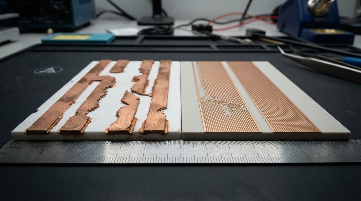
Knowing how to etch copper on ceramic is essential when moving from FR-4 to ceramic substrates — the subtractive principle is the same (apply photoresist, expose, dissolve unwanted copper), but the ceramic base changes several critical variables. The substrate is brittle, the copper bonding mechanism differs between DPC and DBC, and etchant chemistry must be matched to copper thickness to avoid undercutting or ceramic attack. This guide walks through the full process for etching copper on ceramic, etchant options, and the failure modes that catch engineers transitioning from organic boards.
Why Etching Copper on Ceramic Differs from FR-4
On an FR-4 board, copper foil is laminated onto a flexible resin-glass composite. The substrate absorbs minor handling stress, and the copper-resin bond is mechanical. On a ceramic substrate, the copper layer is bonded through one of two fundamentally different methods:
- DBC (Direct Bonded Copper): A copper foil (typically 127–500 µm thick) is bonded to the ceramic at roughly 1065 °C using a controlled Cu-O eutectic layer. The result is a thick, strongly adhered copper sheet that requires aggressive etching and longer dwell times.
- DPC (Direct Plated Copper): A thin seed layer (Ti/Cu or Cr/Cu, sputtered at ~0.1–0.3 µm) is built up by electroplating to a final thickness of 1–100 µm. The thinner copper etches faster and enables finer trace resolution, but the seed layer must also be removed cleanly.
The ceramic itself — whether 96% alumina DBC or alumina DPC — is chemically inert to standard copper etchants. That is an advantage: the etchant stops at the ceramic surface. But the brittleness of Al₂O₃ and AlN means mechanical handling during wet processing must be careful. A dropped panel cracks; it does not flex.
How to Etch Copper on Ceramic: Step-by-Step Process
1. Surface Cleaning
Degrease the copper surface with a mild alkaline cleaner (pH 10–11) or a micro-etch (sodium persulfate at 50–100 g/L, 25–35 °C) to remove oxides and organic residue. The goal is a uniformly wettable surface for photoresist adhesion. Rinse with DI water and dry with filtered nitrogen.
2. Photoresist Application
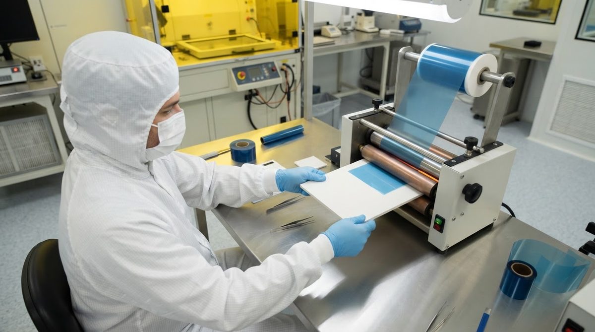
Apply a dry-film photoresist (typical thickness 15–50 µm) by hot-roll lamination at 100–110 °C. For DPC substrates with copper under 20 µm, a thinner resist (15–25 µm) is adequate and improves resolution. Liquid photoresist (spin-coated) is used for features below 30 µm line/space but adds process complexity.
3. Exposure and Development
Expose through a photomask using a UV source (350–420 nm, typically 365 nm i-line). Exposure energy depends on resist thickness — 60–120 mJ/cm² is a common range for 25 µm dry film. Develop in 0.8–1.2% sodium carbonate solution at 28–32 °C. Over-development lifts fine features; under-development leaves resist residue that blocks etching.
4. Etching
This is where copper thickness dictates everything. See the etchant selection table below. Immerse or spray the panel in etchant until all exposed copper is removed. For DPC substrates, the thin seed layer (Ti or Cr) requires a separate etch step after the bulk copper is removed — typically dilute HF (1–5%) for Ti or alkaline permanganate for Cr.
5. Resist Stripping
Strip remaining photoresist in 2–5% NaOH at 45–55 °C. Inspect under magnification for resist residue on trace edges.
6. Final Clean and Inspection
Rinse thoroughly. Inspect trace geometry under optical microscopy or AOI. Measure etch undercut with a cross-section or profilometer. For substrates heading to assembly, the next step is typically a solderable surface finish such as ENIG or OSP.
Enter your copper thickness, etchant type, and target line/space below to estimate etch time and expected undercut for your ceramic substrate.
Etchant Chemistry: Which Solution for Which Copper
| Etchant | Concentration | Temp (°C) | Etch Rate (µm/min) | Best For | Notes |
|---|---|---|---|---|---|
| Ferric chloride (FeCl₃) | 38–42° Baumé | 45–55 | 20–40 | DBC (thick Cu) | Most common. Etch rate drops as Cu loading rises; monitor specific gravity. |
| Cupric chloride (CuCl₂) | 2.0–2.5 N HCl base | 48–55 | 25–50 | DBC and DPC | Regenerable with HCl + oxidiser. Tighter etch factor than FeCl₃. |
| Ammoniacal (alkaline) | NH₃/NH₄Cl, pH 8.0–8.5 | 45–50 | 15–30 | DPC (thin Cu) | Lower undercut on fine lines. Attacks tin resist — use dry film only. |
| Sodium persulfate | 150–250 g/L | 40–50 | 5–15 | Lab / prototype | Gentle, easy to handle. Too slow for production DBC panels. |
Typical values from published etchant supplier data (MacDermid Alpha, Atotech). Confirm rates against your specific chemistry lot and equipment.
Worked Example: Estimating Etch Time for a 300 µm DBC Panel
Understanding how to etch copper on ceramic in practice requires accounting for thickness, chemistry, and undercut. Assume a 300 µm (0.3 mm) DBC copper layer on 96% alumina, etched in ferric chloride at 50 °C with a spray etch rate of 30 µm/min.
Minimum etch time = 300 µm ÷ 30 µm/min = 10 minutes.
Add a 10–15% over-etch margin to clear copper from edges and low-flow zones: practical target is 11–11.5 minutes. At an etch factor of roughly 3:1 (vertical etch : lateral undercut), expect about 100 µm of undercut per side. That means a trace drawn at 500 µm on the photomask will finish at approximately 300 µm. Design your mask artwork with this compensation in mind.
Compare this to a 20 µm DPC copper layer: etch time drops to under 1 minute, undercut falls below 7 µm per side, and 75 µm line/space becomes achievable. This is why DPC dominates fine-pitch ceramic circuits.
Common Etching Defects and How to Prevent Them
Undercut Exceeding Spec
Cause: over-etching, etchant temperature too high, or exhausted chemistry with slow vertical etch rate. Fix: tighten etch time control, monitor etchant specific gravity, and switch to cupric chloride or ammoniacal etchant for better etch factor on fine features.
Copper Residue Between Traces
Cause: under-etching, poor spray coverage, or resist scum blocking etchant contact. Fix: verify develop step completeness, increase spray pressure, and extend etch time by 5–10% while monitoring undercut.
Delamination of Copper from Ceramic
On DBC substrates, delamination during etching is rare because the Cu-O bond is strong. On DPC substrates, aggressive etchants or excessive agitation can undermine the Ti/Cu seed layer at trace edges, lifting copper. Reduce agitation and confirm seed-layer adhesion (peel strength ≥ 6 N/cm per IPC-TM-650, method 2.4.8) before running production etch.
Ceramic Surface Staining
Ferric chloride can leave a brown iron-oxide stain on exposed alumina. This is cosmetic but alarming to inspection teams. A brief dip in 5–10% HCl after etching removes it. AlN substrates are more sensitive — prolonged contact with acidic etchants can slowly hydrolyse AlN. Keep etch times short and rinse immediately.
DPC vs DBC: Which Is Easier to Etch?
When deciding how to etch copper on ceramic, the metallisation method largely determines your process window. The table below summarises the practical differences.
| Parameter | DPC (Direct Plated Copper) | DBC (Direct Bonded Copper) |
|---|---|---|
| Typical Cu thickness | 1–100 µm | 127–500 µm |
| Etch time (FeCl₃, 50 °C) | < 1–3 min | 4–17 min |
| Achievable line/space | 30–75 µm | 200–500 µm |
| Undercut per side | < 10 µm | 50–170 µm |
| Seed layer removal needed | Yes (Ti or Cr etch step) | No |
| Handling risk (breakage) | Moderate (thinner substrates common) | Lower (thicker assemblies) |
Ranges based on typical production parameters. Actual values depend on equipment, chemistry freshness, and substrate geometry.
For power modules carrying hundreds of amps, DBC’s thick copper is necessary despite the coarser etch resolution. For RF circuits, sensor arrays, and LED packages where fine traces matter, DPC is the clear choice. If you are unsure which metallisation suits your design, the guide on metallized ceramic substrates compares all options.
When Not to Use Subtractive Etching
Subtractive etching is not always the right patterning method for ceramic substrates. Even once you know how to etch copper on ceramic properly, consider alternatives in these cases:
- Traces below 30 µm line/space: Additive patterning (semi-additive process or lift-off) gives better resolution than etching, especially on DPC.
- Very thick copper (> 500 µm): Etch times become impractical and undercut uncontrollable. Mechanical milling or pre-formed copper inlays bonded by AMB or DBC are more practical.
- Prototype quantities with fast turnaround: Laser ablation of thin copper layers avoids photomask tooling entirely. It is slower per panel but eliminates setup cost for a single-piece ceramic PCB order.
- Thick-film metallisation (Ag, Au, PdAg): These are screen-printed additively. There is no copper to etch. If your circuit uses gold metallisation, the patterning step happens at printing, not etching.
Frequently Asked Questions
Does ferric chloride attack the ceramic substrate?
No. Alumina (Al₂O₃) and aluminum nitride (AlN) are chemically resistant to ferric chloride at etching concentrations and temperatures. The etchant dissolves copper and stops at the ceramic surface. AlN can slowly hydrolyse in prolonged acid contact, so rinse promptly.
Can I etch a DBC ceramic board with a hobby etching tank?
Technically yes, but results will be poor. DBC copper is 127–500 µm thick — far thicker than the 18–35 µm foil on hobby FR-4 boards. Etch times exceed 10 minutes in a static bath, and without spray agitation, undercut will be severe and uneven. A spray etcher with temperature control is the minimum for repeatable DBC results.
How do I remove the Ti seed layer after etching DPC copper?
A short dip (30–90 seconds) in dilute hydrofluoric acid (1–5% HF) dissolves the titanium adhesion layer without damaging alumina. Use appropriate HF safety protocols — fume hood, face shield, and HF-rated gloves. For chromium seed layers, alkaline permanganate is the standard stripper.
What etch compensation should I add to my artwork?
A practical starting rule: add one copper-thickness worth of compensation per side. For 300 µm DBC copper, widen each trace edge by 300 µm on the photomask (600 µm total). For 20 µm DPC copper, add 20 µm per side. Then run a test panel and measure actual undercut to fine-tune. Etch factor varies with chemistry and equipment.
Is alkaline etchant better than ferric chloride for ceramic substrates?
Alkaline (ammoniacal) etchant gives a higher etch factor — meaning less undercut relative to depth — which matters for fine-pitch DPC circuits. However, it is harder to control (pH and ammonia concentration drift) and attacks tin-based etch resists. For thick DBC copper where resolution is less critical, ferric chloride is simpler and cheaper to operate.