Thick film prints conductors and resistors onto a ceramic substrate using screen-printed pastes fired at 850–1000 °C, producing traces typically 100–250 µm wide and 10–25 µm thick. Thin film deposits metal by sputtering or evaporation in vacuum, then patterns it photolithographically, achieving line widths down to 10–25 µm with film thicknesses of 0.1–2 µm. Choose thick film when you need low cost and embedded resistors; choose thin film when you need fine lines, tight tolerances, or RF-frequency performance.
Key Takeaways
- Thin film achieves 10–25 µm line/space; thick film is limited to roughly 100–250 µm line/space on standard screens.
- Thick film pastes can embed resistors (1 Ω to 10 MΩ per square) directly on the substrate, eliminating discrete components.
- Thin film resistor tolerance can reach ±0.1% after laser trimming, versus ±1–5% for thick film resistors (per Vishay thick/thin film application notes).
- Thick film tooling costs are lower—screens cost a fraction of thin film photomasks and vacuum chamber time.
- For frequencies above 10 GHz, thin film’s smoother conductor surfaces (Ra < 0.1 µm) reduce skin-effect losses significantly compared to thick film (Ra 1–3 µm).
How Thick Film Works
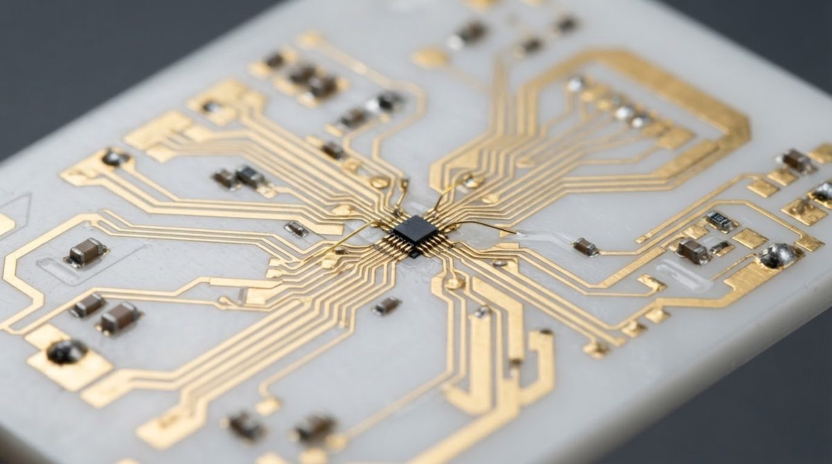
Thick film metallization starts with a stainless-steel or polyester screen stretched over a frame. A squeegee forces a paste—typically a mixture of metal particles (Ag, Au, Pd/Ag, or Pt/Au), glass frit, and organic binder—through the screen’s open pattern onto a fired ceramic substrate, usually 96% Al₂O₃. The printed substrate then passes through a belt furnace at 850–1000 °C. The organic binder burns off, the glass frit melts and bonds the metal to the ceramic, and you are left with a dense conductor 10–25 µm thick.
Resistor pastes (ruthenium oxide or bismuth ruthenate based) can be printed in the same sequence, giving you embedded passives without soldering discrete parts. This is thick film’s single biggest advantage for hybrid circuits. Resistor values are set by the paste’s sheet resistance (available from ~1 Ω/sq to 10 MΩ/sq, per DuPont and Heraeus datasheets) and the printed geometry, then laser-trimmed to the target value. Standard trimmed tolerance is ±1%; ±5% is achievable without trimming. For a deeper look at pricing, see the thick film ceramic cost breakdown.
How Thin Film Works
Thin film metallization happens in a vacuum chamber. A target material—commonly NiCr, TaN, Ti/Pt/Au, or Ti/Cu—is sputtered or evaporated onto a polished ceramic substrate. The resulting film is 0.01–2 µm thick. Circuit patterns are defined by photolithography: spin-coat photoresist, expose through a chrome-on-glass mask, develop, then etch or lift off the unwanted metal. Some processes add electroplated copper or gold on top of the sputtered seed layer to build thickness for higher current capacity.
The photolithographic step is what gives thin film its resolution advantage. Lines and spaces of 10–25 µm are routine; some fabs push below 10 µm on polished AlN or 99.6% Al₂O₃ substrates. Surface finish of the substrate matters: thin film generally requires a polished surface (Ra ≤ 0.05 µm), whereas thick film works on as-fired or lightly lapped substrates. This substrate prep step adds cost.
Thick Film vs Thin Film: Head-to-Head Comparison
| Parameter | Thick Film | Thin Film | Unit / Condition | Source |
|---|---|---|---|---|
| Conductor thickness | 10–25 | 0.01–2 (sputtered); up to 10–20 with plating | µm | Heraeus, Vishay application notes |
| Minimum line/space | 100–250 | 10–25 | µm | Industry standard; CoorsTek design guides |
| Line width tolerance | ±20–30 | ±2–5 | µm | Kyocera thick/thin film specs |
| Conductor surface roughness (Ra) | 1–3 | 0.02–0.1 | µm | Maruwa substrate datasheets |
| Resistor tolerance (trimmed) | ±1–5% | ±0.1–1% | — | Vishay thin film resistor guide |
| Resistor TCR | ±50–200 | ±5–25 | ppm/°C | DuPont, Vishay datasheets |
| Typical paste/target metals | Ag, Au, Pd/Ag, Pt/Au | NiCr, TaN, Ti/Pt/Au, Ti/Cu/Au | — | Heraeus, Materion |
| Substrate surface requirement | As-fired OK (Ra 0.3–0.8 µm) | Polished (Ra ≤ 0.05 µm) | µm | CoorsTek, Kyocera |
| Typical NRE / tooling cost | Low (screens: $50–$300 each) | Higher (masks + vacuum setup: $500–$5,000+) | USD, approximate | Industry estimates |
| Best frequency range | DC to ~5 GHz | DC to 100+ GHz | — | Rogers, Kyocera RF design notes |
Typical values for commercially available material, for comparison only. Confirm against the datasheet for your specific grade.
When to Choose Thick Film
Thick film is the default for cost-sensitive ceramic hybrids, sensor substrates, and power circuits that do not need fine geometry. If your minimum trace is 150 µm or wider and you want embedded resistors or heater elements, thick film is the practical choice. Screen printing scales well in volume: once the screens are made, per-unit cost drops fast.
Automotive sensor modules, LED driver substrates, and thick film heaters for medical or industrial instruments are typical thick film applications. The process also tolerates rougher, less expensive substrates—96% Al₂O₃ as-fired is the workhorse. If your project involves HTCC or LTCC multilayer ceramics, thick film conductor pastes are the standard metallization method for those co-fired structures.
When to Choose Thin Film
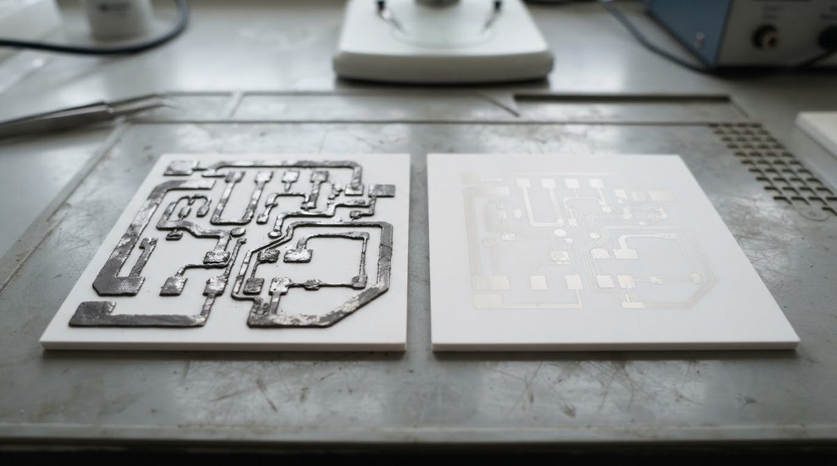
Thin film wins when you need any of the following: line widths below 75 µm, resistor tolerance tighter than ±1%, temperature coefficient of resistance (TCR) below ±25 ppm/°C, or operation above 10 GHz. The smooth conductor surface minimizes skin-effect losses, which matters for millimeter-wave radar, 5G antenna feed networks, and precision instrumentation.
Thin film is also the process behind DPC (Direct Plated Copper) ceramic PCBs, where a sputtered Ti/Cu seed layer is electroplated up to 10–50 µm of copper and patterned photolithographically. This gives you both the fine-line capability of thin film and the current-carrying capacity of a copper conductor. For a direct comparison of DPC against thin film metallization, see the DPC vs thin film process comparison.
Worked Example: Insertion Loss at 24 GHz
Consider a 50 Ω coplanar waveguide on 99.6% Al₂O₃ (εr ≈ 9.9), 10 mm long. At 24 GHz the skin depth in copper is about 0.42 µm (per δ = √(ρ / πfμ₀), with ρ = 1.68 × 10⁻⁸ Ω·m). A thick film silver conductor with Ra ≈ 2 µm has a surface roughness several times the skin depth, increasing effective resistivity by a factor of 1.5–2× (per the Hammerstad–Jensen roughness model). A thin film copper conductor with Ra ≈ 0.05 µm adds negligible roughness loss. Over 10 mm, this difference translates to roughly 0.15–0.3 dB of extra insertion loss for the thick film line. In a phased-array feed network with dozens of such segments, that penalty compounds quickly.
Combining Both Processes on One Substrate
Some hybrid designs use both. A common approach: thick film prints the resistor layer, then thin film deposits the precision conductor pattern on top or on the opposite face. This captures embedded passives from thick film and fine geometry from thin film. The trade-off is two separate metallization sequences, which increases process cost and cycle time. It is justified mainly in high-reliability military or aerospace hybrids where component count reduction outweighs fabrication cost.
When Not to Use Either Process
If your design needs copper thickness above 300 µm for high-current power modules (IGBTs, SiC MOSFETs), neither thick film nor thin film is the right starting point. Look at DBC vs DPC or AMB vs DPC instead—those processes bond or plate bulk copper onto ceramic for current ratings that paste or sputtered films cannot match.
If your board is a standard digital or mixed-signal design operating below 125 °C with no special thermal or dielectric requirements, FR-4 or metal-core PCB will cost a fraction of any ceramic process. Ceramic metallization—thick or thin film—makes economic sense only when the substrate’s thermal conductivity, dielectric properties, or operating temperature justify it.
FAQ
Can thick film and thin film be used on aluminum nitride (AlN)?
Yes. Thick film pastes formulated for AlN are available from Heraeus and DuPont, though the paste chemistry differs from Al₂O₃ formulations because AlN reacts with standard glass frits. Thin film sputtering works well on polished AlN and is common for high-power RF and laser diode submounts.
Which process is faster for prototypes?
Thick film is usually faster. Screens can be made in a day or two, and the print-fire cycle takes hours. Thin film requires photomask fabrication and vacuum deposition scheduling, adding several days to a week. For quick-turn evaluation, thick film is the lower-friction path if your geometry allows it.
Do thick film conductors handle as much current as thin film?
Thick film conductors are 10–25 µm of printed metal, so their cross-sectional area is larger than a 0.1–1 µm sputtered thin film trace of the same width. However, thin film processes that include electroplated copper can build up to 20–50 µm, matching or exceeding thick film current capacity. Compare cross-sectional area and resistivity, not just the process name.
Is thin film always more expensive?
At low volumes, yes—vacuum deposition, photomasks, and substrate polishing all add cost. At very high volumes with automated sputtering lines, the per-unit gap narrows, but thin film still costs more than thick film for equivalent complexity. The cost premium is typically 2–5× depending on layer count and feature size.
What is the typical operating temperature limit for each process?
Thick film conductors, once fired at 850–1000 °C, are stable in continuous service up to roughly 300–500 °C depending on paste system. Thin film metallizations (Ti/Pt/Au) can operate above 300 °C as well, but adhesion and interdiffusion become concerns above 400 °C without barrier layers. Both processes far exceed the limits of organic PCB materials.
Next Step
If you have narrowed your choice to one process but need to confirm it against your specific layout, substrate, and volume, request a quote with your Gerber files. The fabrication review will flag any features that push beyond the process limits discussed here.