Aluminum nitride (AlN) conducts heat roughly 6–8× better than 96% alumina (Al₂O₃)—170–200 W/m·K versus 24–28 W/m·K at 25 °C—but it costs three to five times more per square centimetre of finished substrate. That single ratio drives most of the decision between the two materials. Everything below helps you decide whether the thermal gain justifies the price for your specific board.
Key Takeaways
- AlN thermal conductivity: 170–200 W/m·K at 25 °C (per Kyocera SN-220 and Maruwa AN-200 datasheets). Al₂O₃ 96%: 24–28 W/m·K at 25 °C (per CoorsTek ADS-96R datasheet).
- AlN CTE (4.5–5.0 ppm/°C) is a closer match to silicon (2.6 ppm/°C) and SiC (4.0 ppm/°C) than alumina’s 7.0–8.0 ppm/°C, reducing die-attach fatigue in power cycling.
- 96% alumina substrates cost roughly $0.03–$0.08/cm² in volume; AlN runs $0.15–$0.40/cm² depending on grade and surface finish.
- Alumina is the right default. Switch to AlN only when thermal resistance, CTE match, or high-frequency loss tangent forces you to.
- Both materials are compatible with DBC, DPC, and thick-film metallisation. AlN requires an oxidation step before thick-film printing to ensure adhesion.
Material Properties: AlN vs Alumina Side by Side
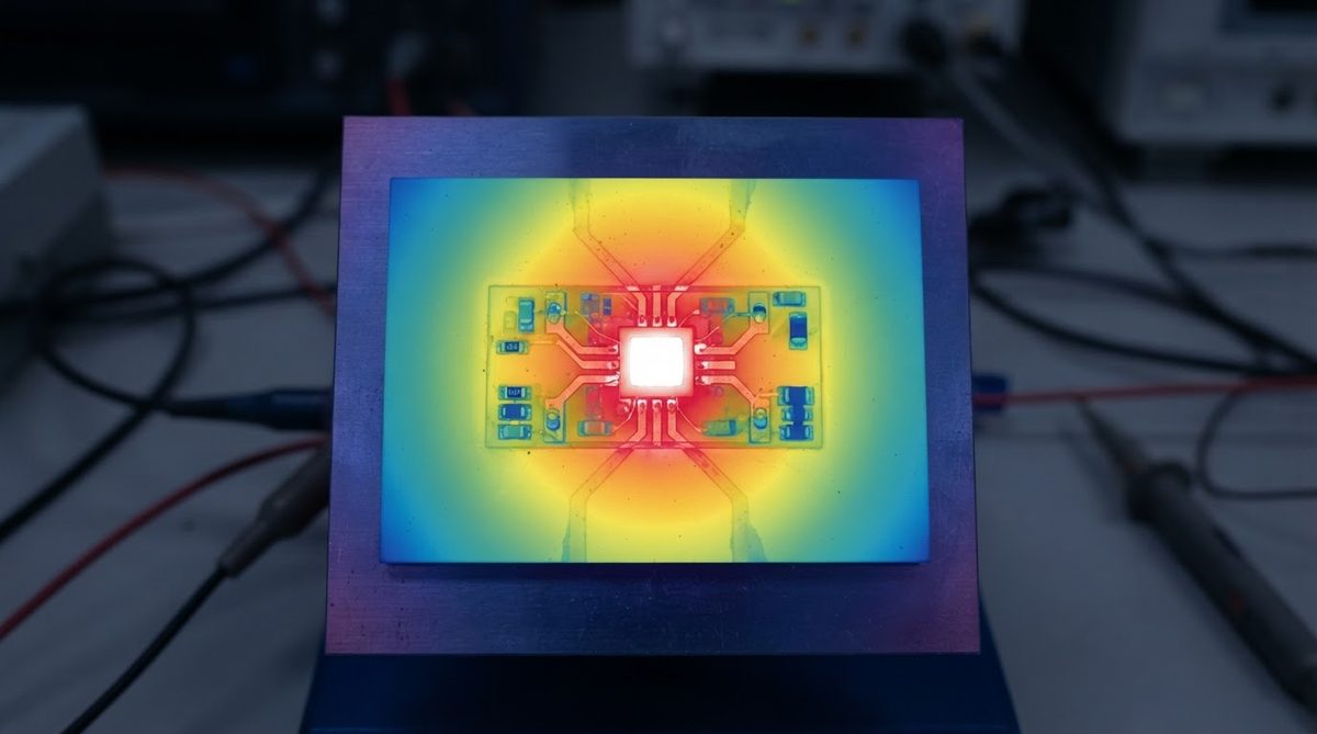
| Parameter | 96% Al₂O₃ | AlN | Unit | Condition | Source |
|---|---|---|---|---|---|
| Thermal conductivity | 24–28 | 170–200 | W/m·K | 25 °C, ASTM E1461 | CoorsTek ADS-96R / Kyocera SN-220 |
| CTE | 7.0–8.0 | 4.5–5.0 | ppm/°C | 25–400 °C, ASTM E228 | CoorsTek / Maruwa |
| Dielectric constant (εr) | 9.0–9.5 | 8.5–9.0 | — | 1 MHz, 25 °C | CoorsTek / Kyocera |
| Loss tangent (tan δ) | 0.0002–0.0010 | 0.0003–0.0005 | — | 1 MHz, 25 °C | CoorsTek / Kyocera |
| Flexural strength | 350–380 | 300–350 | MPa | ASTM C1161, 3-pt bend | CoorsTek / Maruwa |
| Volume resistivity | >10¹⁴ | >10¹⁴ | Ω·cm | 25 °C | CoorsTek / Kyocera |
| Max use temperature | 1 600 | 1 000 (in air, oxidation limit) | °C | Continuous | Maruwa / CeramTec |
| Typical substrate cost | 0.03–0.08 | 0.15–0.40 | $/cm² | Volume, DPC-ready, 0.635 mm | Industry pricing 2024 |
Typical values for commercially available material, for comparison only. Confirm against the datasheet for your specific grade.
The numbers that matter most for substrate selection are thermal conductivity, CTE, and cost. Dielectric constant and loss tangent are close enough that they rarely decide the contest below 10 GHz. Above 10 GHz, AlN’s lower tan δ starts to matter for millimetre-wave circuits. For a broader look at how these two ceramics stack up against other substrates, see the alumina 96% vs aluminum nitride substrate comparison.
Thermal Performance: A Worked Example
Consider a GaN HEMT dissipating 50 W through a 25 × 25 mm substrate that is 0.635 mm thick. The one-dimensional conduction resistance through the substrate is:
Rth = t / (k × A)
For 96% alumina (k = 25 W/m·K):
Rth = 0.000635 / (25 × 0.000625) = 0.0406 °C/W
ΔT through substrate = 50 W × 0.0406 °C/W = 2.03 °C
For AlN (k = 180 W/m·K):
Rth = 0.000635 / (180 × 0.000625) = 0.00564 °C/W
ΔT through substrate = 50 W × 0.00564 °C/W = 0.28 °C
The difference is 1.75 °C. On a 25 × 25 mm footprint at 50 W that gap looks small. Now shrink the die to 5 × 5 mm (A = 0.000025 m²) at the same 50 W:
Alumina: Rth = 0.000635 / (25 × 0.000025) = 1.016 °C/W → ΔT = 50.8 °C
AlN: Rth = 0.000635 / (180 × 0.000025) = 0.141 °C/W → ΔT = 7.06 °C
At high power density—small die, high wattage—AlN saves 43 °C through the substrate alone. That is the regime where AlN pays for itself. At low power density, the substrate is not the thermal bottleneck, and the extra cost of AlN buys almost nothing.
CTE Match: Why It Matters for Die Attach
Silicon has a CTE of about 2.6 ppm/°C. SiC is around 4.0 ppm/°C. GaN-on-SiC sits in the same range. AlN at 4.5–5.0 ppm/°C is a much closer match to these die materials than alumina at 7.0–8.0 ppm/°C.
A large CTE mismatch between the die and the substrate generates shear stress in the solder or sinter layer during thermal cycling. Over thousands of power cycles (as defined by JEDEC JESD22-A104), that stress nucleates cracks. The closer the CTE match, the longer the joint survives. For bare-die attach of SiC MOSFETs or GaN HEMTs, AlN extends power-cycle life significantly compared to alumina—often by 2–5× at ΔTj = 100 °C, depending on joint material and thickness.
If your device is packaged (e.g., a QFN or TO-263), the package body and leadframe dominate the CTE interaction with the board. In that case, the substrate CTE matters less, and alumina is usually sufficient. For a comparison with another substrate that excels in power-cycling endurance, see Si₃N₄ vs AlN for power modules.
Cost Drivers: What Makes AlN Expensive
AlN powder costs more than alumina powder. Sintering AlN requires a nitrogen atmosphere and higher purity control to prevent oxygen contamination, which degrades thermal conductivity. Machining and laser scribing are harder because AlN is tougher on tooling. Yield rates for AlN substrates are lower, especially at thicknesses below 0.38 mm.
Expect these rough cost multiples for a finished, metallised substrate in the same geometry:
- Raw substrate (no metallisation): AlN is 3–5× the cost of 96% alumina.
- DBC (direct bond copper): AlN DBC is 2–4× the cost of alumina DBC, because copper bonding yield on AlN is lower.
- DPC (direct plated copper): AlN DPC is roughly 2–3× the cost of alumina DPC. The oxidation pre-treatment adds a step.
Volume helps. At 10 000+ pieces, the AlN premium narrows toward the low end of those ranges. At prototype quantities (under 50 pieces), the premium can exceed 5×. If you are evaluating costs for a ceramic board, the ceramic PCB comparison hub covers all substrate options in one place.
Metallisation Compatibility
Both AlN and alumina work with the major ceramic metallisation processes: DBC, DPC, thick film, and thin film. The practical differences:
| Process | Alumina | AlN | Notes |
|---|---|---|---|
| DBC | Standard, high yield | Requires controlled oxidation layer | AlN DBC is well-established but lower yield |
| DPC | Standard | Standard with pre-oxidation | Both produce fine-line traces (<50 µm) |
| Thick film (Ag, Au, Cu pastes) | Standard | Needs oxide adhesion layer | AlN thick-film adhesion is weaker without proper surface prep |
| Thin film (sputtered Ti/Cu, TaN) | Standard | Standard | Both substrates suit thin-film resistor networks |
| AMB (active metal brazing) | Uncommon, not needed | Common for thick copper (>0.3 mm) | AMB on AlN is the standard for high-reliability power modules |
For a deeper look at how DPC and thin-film processes compare on either substrate, see the DPC vs thin film process guide.
RF and High-Frequency Considerations
Below 6 GHz, the difference in εr (9.0–9.5 for alumina vs 8.5–9.0 for AlN) and tan δ is small enough that alumina is the standard RF substrate material. It is cheaper and well-characterised for microstrip and coplanar waveguide designs.
Above 10 GHz—particularly in 5G mmWave (24–40 GHz) and radar (77 GHz)—AlN’s slightly lower loss tangent reduces insertion loss. At 77 GHz, even a difference of 0.0003 in tan δ can add up over a multi-section filter or feed network. That said, if RF loss is your primary concern, you may also want to evaluate low-loss glass or fused quartz substrates, which have εr values in the 3.8–4.5 range and tan δ below 0.0001. The ceramic vs glass substrate comparison covers that trade-off.
When NOT to Use AlN
AlN is overkill—and a waste of budget—in these situations:
- Power density below ~5 W/cm². The substrate is not the thermal bottleneck. Alumina, or even FR-4 in some cases, handles the heat fine.
- Packaged devices on the board. The package thermal resistance dominates. CTE match to the die is irrelevant because you are soldering to leads, not to bare silicon.
- Cost-sensitive, high-volume consumer products. If the BOM target is under $0.50 for the substrate, AlN cannot compete.
- Large panel sizes. AlN substrates are typically available up to about 114 × 114 mm (Maruwa) or 139.7 × 190.5 mm (Kyocera). If your board exceeds those dimensions, alumina or an MCPCB is more practical.
- Environments above 1 000 °C in air. AlN oxidises. Alumina is stable to 1 600 °C.
When AlN Is the Right Call
Choose AlN when your design hits one or more of these conditions:
- Bare-die attach of SiC, GaN, or Si power devices with ΔTj cycling above 80 °C.
- Thermal flux density above 10 W/cm² through the substrate.
- Junction temperature budget is tight and every degree counts (e.g., high-reliability automotive inverters, aerospace power converters).
- mmWave RF circuits above 20 GHz where substrate loss tangent affects system noise figure.
If your application demands even higher mechanical toughness and thermal-cycling endurance than AlN provides—at the cost of slightly lower thermal conductivity (70–90 W/m·K)—silicon nitride (Si₃N₄) is the next material up the reliability ladder. See the AlN vs Si₃N₄ substrate comparison for that decision.
Decision Framework: A Quick Checklist
Run through these five questions for your board. If you answer “yes” to two or more, AlN is worth quoting.
- Is the die bonded directly to the substrate (no package)?
- Does thermal flux through the substrate exceed 10 W/cm²?
- Does the product undergo more than 1 000 power cycles with ΔTj > 80 °C over its lifetime?
- Is the operating frequency above 20 GHz?
- Is the total substrate area small enough (<25 cm²) that the AlN cost premium is under $5 per board?
If every answer is “no,” alumina is almost certainly the better choice. Save the budget for thicker copper, better thermal interface material, or a larger heat sink.
Frequently Asked Questions
Can I use the same Gerber files for AlN and alumina substrates?
Yes. The Gerber data defines the copper pattern, not the substrate material. You can send the same artwork for both and specify the substrate on your purchase order or fabrication drawing. Panel size limits may differ, so confirm maximum substrate dimensions with your fabricator.
Does AlN need a special solder paste?
No. Standard SAC305 or SnAgCu solders work on metallised AlN substrates. The metallisation layer (typically Ni/Au or Ni/Ag over Cu) is what the solder wets to, not the ceramic itself. For high-temperature operation above 250 °C, consider high-lead (Pb93.5Sn5Ag1.5) or sintered silver die attach instead.
Is AlN safe to handle without special precautions?
Sintered AlN substrates are safe to handle with standard ESD and cleanroom practices. Unlike beryllium oxide, AlN dust is not classified as a carcinogen. Machining or grinding AlN does produce fine dust that can irritate the respiratory tract, so use dust extraction and a particulate mask during those operations.
How does humidity affect AlN?
AlN reacts slowly with moisture to form aluminum hydroxide on the surface, which degrades thermal conductivity at the interface. In high-humidity environments, AlN substrates should be stored in dry nitrogen packaging and used within the manufacturer’s recommended shelf life. Metallised and assembled AlN boards are largely protected by the metal layers and encapsulant.
Can I get AlN in thicknesses below 0.38 mm?
Yes. Kyocera and Maruwa both offer AlN substrates down to 0.25 mm. Thinner substrates reduce thermal resistance further but are more fragile and harder to handle during assembly. Below 0.25 mm, yield drops and lead times increase significantly.
Next Step
If your thermal model shows that alumina’s conductivity is not enough, request a quote for both materials in your geometry. Comparing the actual price delta against the thermal gain is the fastest way to close the decision. Choosing between silver and copper metallisation is often the next question once you have picked your substrate.