DPC (Direct Plated Copper) and thin film are closely related sputtering-based metallization processes for ceramic substrates, but they serve different design points. DPC uses a sputtered seed layer followed by pattern plating to build copper up to 100–300 µm, targeting power and thermal applications. Thin film stays in the sub-10 µm range, using photolithography and etching on the sputtered metal stack to achieve line/space down to 10–20 µm for RF, sensor, and precision resistor circuits. Choosing between them comes down to whether your design is constrained by current capacity or feature resolution.
Key Takeaways
- DPC and thin film both start with a sputtered adhesion/seed layer (typically Ti/Cu or Cr/Cu) on a ceramic substrate, but diverge after that step.
- DPC builds copper to 50–300 µm via electroplating, supporting current loads above 10 A per trace on compact ceramic boards.
- Thin film keeps total metal thickness under 10 µm and achieves line/space as fine as 10/10 µm, roughly 3–5× finer than DPC.
- Thin film costs 2–4× more per panel than DPC at equivalent substrate size, driven by cleanroom processing and tighter lithography.
- Many designs that need moderate resolution (50/50 µm) and moderate copper (20–50 µm) can go either way; DPC is usually the more economical choice in that overlap zone.
How DPC and Thin Film Actually Work
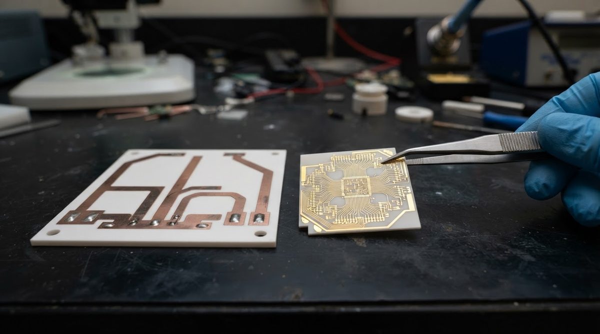
Both processes begin the same way: a ceramic substrate (typically 96% or 99.6% Al₂O₃, or AlN) is cleaned and loaded into a vacuum chamber where a sputtered seed layer of Ti/Cu or Cr/Cu is deposited. This seed layer is usually 0.1–0.5 µm thick and provides the adhesion and conductivity needed for the next steps. After sputtering, the two processes diverge sharply.
DPC Process Flow
A photoresist is applied and patterned to expose the areas where copper is wanted. Copper is then electroplated through the resist openings, building thickness from 20 µm up to 200–300 µm depending on the design. After plating, the resist is stripped and the exposed seed layer is etched away, leaving isolated copper features. The minimum practical line/space for DPC is around 30/30 µm to 50/50 µm, limited by the plating aspect ratio and undercut during seed-layer etching. For a deeper look at how electroplated and electroless copper compare on ceramic, see the dedicated comparison.
Thin Film Process Flow
Instead of plating through a resist, thin film deposits the full metal stack by sputtering or evaporation—often a multi-layer structure such as Ti/Pt/Au, Cr/Ni/Au, or Ti/Cu/Ni/Au—then patterns it subtractively using photolithography and wet or dry etching. Total conductor thickness stays below 10 µm, often 1–5 µm. Because there is no plating step, line/space is set by the lithography resolution, typically 10/10 µm to 25/25 µm. Thin film can also deposit resistor materials (TaN, NiCr) in the same process, enabling integrated precision resistors with ±1% tolerance or better. Detailed design rules for thin film ceramic PCBs cover the full set of constraints.
DPC vs Thin Film: Head-to-Head Spec Comparison
| Parameter | DPC | Thin Film | Unit | Notes |
|---|---|---|---|---|
| Seed layer method | Sputtering | Sputtering / evaporation | — | Same starting point |
| Copper build-up | Electroplating | Sputtering (subtractive pattern) | — | Key process divergence |
| Conductor thickness | 20–300 | 0.5–10 | µm | DPC can go thicker for high current |
| Min line / space | 30/30 – 50/50 | 10/10 – 25/25 | µm | Thin film limited by lithography, DPC by plating |
| Positional accuracy | ±10–15 | ±5–10 | µm | Thin film uses stepper or mask aligner |
| Integrated resistors | No (external only) | Yes (TaN, NiCr) | — | Thin film deposits resistor layer in-process |
| Current handling (1 mm trace) | 5–15 A (at 100 µm Cu) | 0.5–2 A (at 5 µm Cu) | A | Depends on thermal environment |
| Typical substrate | Al₂O₃ 96%, AlN | Al₂O₃ 99.6%, AlN, quartz | — | Thin film often needs smoother surface (Ra < 0.1 µm) |
| Relative cost per panel | 1× | 2–4× | — | Driven by cleanroom, lithography, and multi-layer sputtering |
Typical values for commercially available processes, for comparison only. Confirm against the datasheet for your specific grade and vendor.
Worked Example: Choosing a Process for a 10 W LED Driver
Suppose you are designing a 25 × 25 mm ceramic LED driver board. The design has 8 traces carrying 2 A each, minimum line/space of 75/75 µm, and no integrated resistors. Total power dissipation is 10 W.
DPC path: 50 µm copper on 96% Al₂O₃ (0.635 mm thick). A 0.3 mm wide trace at 50 µm copper handles 2 A comfortably per IPC-2152 derating. 75/75 µm line/space is well within DPC’s 30/30 µm capability. Estimated panel cost: 1×.
Thin film path: 5 µm copper on 99.6% Al₂O₃. A 0.3 mm trace at 5 µm copper handles roughly 0.8 A before thermal limits—you would need to widen traces to ~0.8 mm, eating board area. The finer resolution of thin film is wasted at 75/75 µm. Estimated panel cost: 2.5×.
Verdict: DPC wins here on cost, current capacity, and simplicity. Thin film adds nothing this design needs. For more on what drives thin film ceramic cost, see the cost breakdown page.
When Thin Film Wins Over DPC
Thin film is the right process when your design demands one or more of the following:
- Fine features below 30 µm line/space. RF matching networks, mmWave filters, and interdigital capacitors routinely need 10–20 µm features that DPC cannot resolve.
- Integrated thin-film resistors. Depositing TaN or NiCr resistors directly on the substrate eliminates discrete components and improves matching in sensor bridges and precision analog front-ends.
- Tight positional accuracy. Flip-chip bonding pads for bare die with sub-100 µm pitch benefit from thin film’s ±5 µm placement accuracy.
- Multi-metal stacks. Ti/Pt/Au or Cr/Ni/Au stacks for wire-bonding or hermetic sealing are native to thin film but awkward to achieve with DPC’s plating-centric flow.
Typical applications include RF/microwave modules, MEMS sensor substrates, hybrid thick/thin film circuits, and medical implant electronics. The 99.6% alumina thin film substrate page covers the material specs most commonly paired with this process.
When DPC Wins Over Thin Film
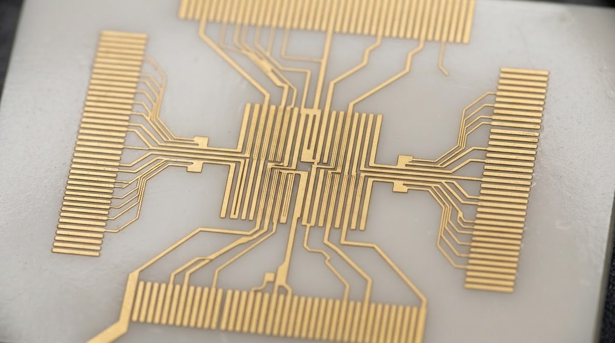
DPC is the better choice when current capacity and thermal spreading matter more than feature size. Power converters, high-brightness LED arrays, and IGBT driver boards all benefit from 50–200 µm copper on ceramic. DPC also costs less per panel and has shorter cycle times because it skips the cleanroom lithography and multi-target sputtering runs that thin film requires.
If your design sits in the overlap zone—50/50 µm features, 20–50 µm copper—DPC is almost always the more economical default. Reserve thin film for the designs that genuinely need it.
When Not to Use Either Process
Neither DPC nor thin film is the right answer in every situation. Consider alternatives when:
- Copper thickness above 300 µm is required. DBC (Direct Bond Copper) and AMB (Active Metal Brazing) bond pre-formed copper foils 0.3–0.8 mm thick to ceramic. For power modules needing that level of current and thermal spreading, DBC or AMB is the standard approach.
- Cost must be minimized on a simple, low-density layout. Thick-film screen printing is cheaper than both DPC and thin film for circuits with line/space above 100 µm. See the thick film versus thin film comparison for a detailed breakdown.
- Multilayer structures with embedded vias are needed. HTCC and LTCC co-fire processes build true 3D ceramic circuits. Neither DPC nor thin film produces buried vias in a monolithic ceramic body.
- FR-4 meets all requirements. If operating temperature stays below 130 °C, thermal conductivity is not a constraint, and standard PCB tolerances suffice, FR-4 at 1/10th the cost is the rational choice.
Frequently Asked Questions
Can DPC and thin film be combined on the same substrate?
Yes. Some hybrid designs use a thin-film resistor or fine-pitch layer on one side and a DPC power layer on the other. This adds process steps and cost, but it lets a single substrate serve both precision analog and power functions.
Does thin film require a smoother substrate than DPC?
Generally, yes. Thin film processes work best on substrates with surface roughness Ra below 0.1 µm (as-fired or lapped and polished), because sub-micron metal layers conform to surface defects. DPC is more tolerant, performing well on as-fired 96% alumina with Ra of 0.3–0.5 µm.
Is DPC the same as sputtered copper?
Not exactly. DPC uses sputtering only for the seed layer (0.1–0.5 µm). The bulk conductor is electroplated copper. A “sputtered copper” board where the full thickness is deposited by sputtering would be classified as thin film, not DPC.
Which process has a shorter lead time?
DPC is typically faster. It requires fewer vacuum deposition steps and no cleanroom lithography, so prototype turnaround is often 1–2 weeks shorter than thin film, depending on the vendor’s queue.
Can I use AlN substrates with both processes?
Yes. Both DPC and thin film are compatible with aluminum nitride. AlN’s higher thermal conductivity (170–200 W/mK) benefits power DPC designs, while its low dielectric loss (tan δ ~0.001 at 1 MHz) suits thin-film RF circuits.
Next Step
If your design needs fine features or integrated resistors, start with the thin film capabilities page to confirm your line/space and metal stack are feasible. For power-oriented layouts, compare DPC against DBC on the ceramic PCB comparison hub. When you are ready to get pricing on either process, request a quote and upload your files directly.