Via filling ceramic PCBs creates a solid electrical and thermal path through the substrate by packing the via barrel with conductive material before or during firing. The dominant methods are co-fired paste fill (used in HTCC and LTCC), post-fire conductive paste fill, and electrolytic copper plating. Each via filling ceramic technique suits different frequency ranges, current loads, and thermal demands. Choosing the wrong one can mean cracked vias after thermal cycling or unacceptable insertion loss above 10 GHz.
Key Takeaways
- Co-fired tungsten or molybdenum paste fill (HTCC) handles operating temperatures above 800 °C but has higher resistivity (~5.5 µΩ·cm for W) than copper-filled alternatives (~1.7 µΩ·cm).
- Electrolytic copper via fill on post-fired substrates gives the lowest via resistance and best thermal conductivity (~390 W/mK) but is limited to substrates that survive the plating chemistry.
- Non-conductive fill with a plated cap is sometimes used for impedance-controlled RF lines on ceramic, keeping the via from acting as a stub.
- Minimum filled-via diameter on ceramic substrates is typically 100–150 µm for laser-drilled holes, versus 75 µm on organic boards.
- Via fill voids above 25% by cross-section area are a common reject criterion per internal quality standards aligned with IPC-6012 Class 3.
Why Via Filling Ceramic Substrates Matters
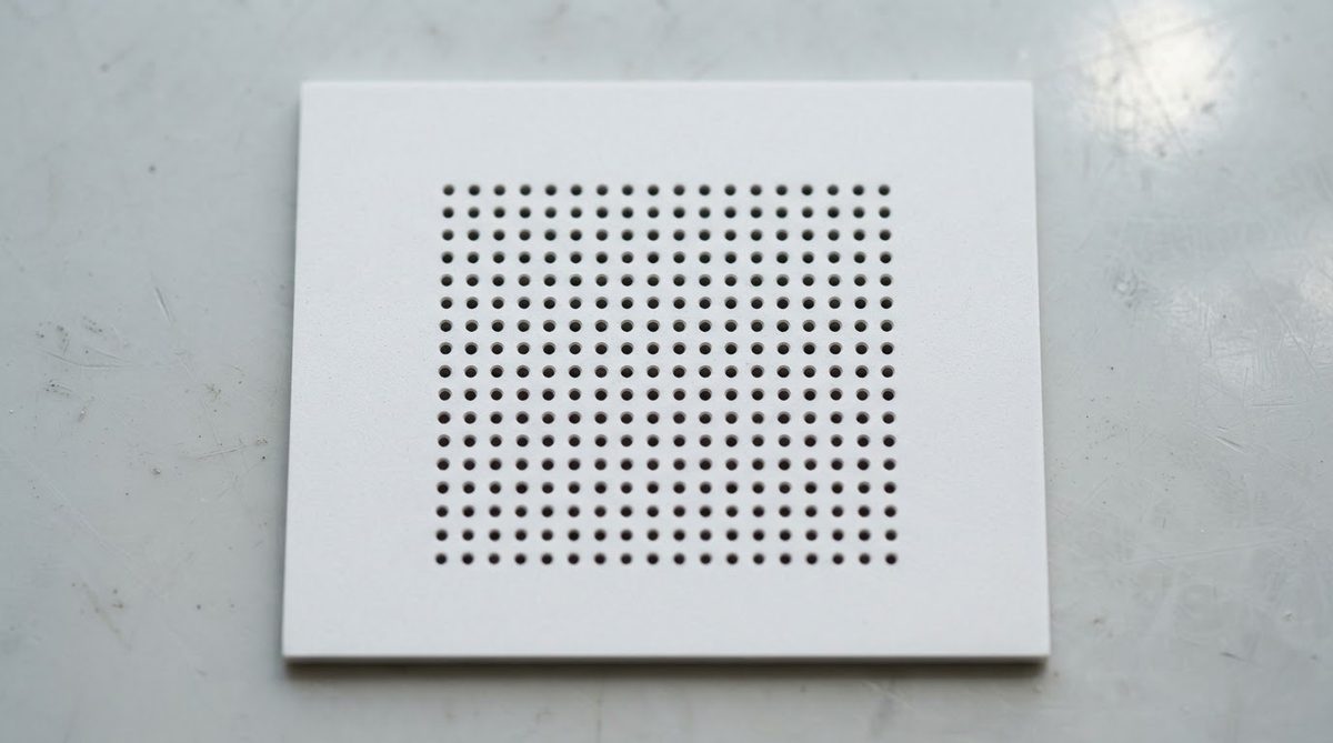
Open (hollow) vias in ceramic substrates trap flux, outgas during reflow, and present a reliability risk in hermetic packages. A filled via eliminates the void, provides a flat pad surface for component mounting, and improves both electrical conductivity and thermal dissipation through the Z-axis. In power electronics, a filled copper via array under a die pad can cut junction-to-case thermal resistance by 30–50% compared to an unfilled array of the same geometry.
For RF and microwave circuits operating above 5 GHz, unfilled vias act as resonant stubs whose length equals the substrate thickness. Via filling ceramic boards with conductive paste or copper lowers the stub’s impedance discontinuity and reduces insertion loss. This matters on alumina and aluminum nitride substrates used in impedance-controlled ceramic designs.
Three Main Via Filling Ceramic Methods
1. Co-Fired Paste Fill (HTCC / LTCC)
In HTCC processing, vias are punched or laser-drilled into green (unfired) tape, then filled with tungsten (W) or molybdenum (Mo) paste using a screen printer or stencil. The filled tape layers are laminated and co-fired at 1,500–1,600 °C. The metal paste sinters simultaneously with the ceramic, producing a monolithic structure. LTCC uses silver or gold paste and fires at 850–900 °C.
Co-fired fills are the most reliable option for multilayer ceramic packages because the fill and substrate shrink together. The trade-off: tungsten’s bulk resistivity is roughly 3× that of copper, so DC resistance per via is higher. For a 200 µm diameter, 635 µm deep tungsten-filled via, DC resistance is approximately 11 mΩ—acceptable for signal routing but worth tracking in high-current arrays.
2. Post-Fire Conductive Paste Fill
For single-layer or DPC (direct plated copper) substrates that are already fired, vias are laser-drilled into the sintered ceramic and then filled with a conductive paste—typically silver-loaded or copper-loaded epoxy. The paste is cured at 150–200 °C. This via filling ceramic approach is simpler than plating but introduces an organic binder that limits the via’s maximum operating temperature to roughly 250–300 °C, well below the ceramic’s own capability. Consult the ceramic maximum temperature guide to understand how fill material limits overall board ratings.
Conductive epoxy fills also have higher resistivity (typically 30–80 µΩ·cm depending on filler loading) and lower thermal conductivity (1–5 W/mK) than solid metal fills. They are a practical choice for low-frequency, moderate-power designs where full copper plating is not justified by the budget.
3. Electrolytic Copper Via Fill
Electrolytic copper plating fills vias from the bottom up using a pulsed or DC plating bath with proprietary leveling and brightening additives. The result is a near-solid copper plug with resistivity close to bulk copper (1.7 µΩ·cm) and thermal conductivity of ~390 W/mK. This method is standard for DPC ceramic substrates and is detailed further in the copper plating capabilities overview.
Copper-filled vias on ceramic require careful control of seed-layer adhesion. Titanium or chromium sputtered adhesion layers must survive the acidic plating bath without delamination. Typical plating time for a 150 µm via in a 380 µm thick Al₂O₃ substrate is 45–90 minutes, depending on current density and bath chemistry.
Enter your substrate material, via diameter, fill type, and operating temperature to see how each method performs under your thermal conditions.
Via Fill Comparison Table
| Parameter | Co-Fired W (HTCC) | Conductive Epoxy | Electrolytic Cu | Unit | Condition / Source |
|---|---|---|---|---|---|
| Bulk resistivity | 5.3–5.6 | 30–80 | 1.7–1.8 | µΩ·cm | 20 °C; CoorsTek / paste vendor datasheets |
| Thermal conductivity | 170–174 | 1–5 | 385–400 | W/mK | 20 °C; Maruwa / paste vendor datasheets |
| Max service temperature | >800 | 250–300 | ~400 (limited by oxidation) | °C | Continuous, in inert or air atmosphere |
| Min via diameter (typical) | 100–150 | 150–200 | 100–150 | µm | Production capability, laser-drilled |
| Void fraction (accept limit) | ≤15% | ≤25% | ≤10% | % area | Cross-section per IPC-6012 Class 3 guidance |
| Hermeticity compatible | Yes | No | Yes (with cap plating) | — | MIL-STD-883 Method 1014 |
Typical values for commercially available materials, for comparison only. Confirm against the datasheet for your specific grade.
Worked Example: Via Resistance and Thermal Path
Assume a 150 µm diameter via through a 380 µm thick 96% alumina substrate, filled with electrolytic copper.
DC resistance:
R = ρ · L / A
ρ = 1.72 × 10⁻⁶ Ω·cm, L = 0.038 cm, A = π × (0.0075 cm)² = 1.77 × 10⁻⁴ cm²
R = (1.72 × 10⁻⁶ × 0.038) / 1.77 × 10⁻⁴ ≈ 0.37 mΩ
Thermal resistance (single via):
R_th = L / (k · A) = 0.0038 m / (390 W/mK × 1.77 × 10⁻⁸ m²) ≈ 0.55 °C/W
An array of 25 such vias under a 3 mm × 3 mm die pad drops the combined thermal resistance to roughly 0.022 °C/W through the via array alone. The ceramic substrate between vias still contributes; for 96% Al₂O₃ at 24–28 W/mK that inter-via resistance is typically 2–5× the via array resistance, so the vias dominate the thermal path as intended.
Design Rules for Via Filling Ceramic Boards
- Via-to-via pitch: Minimum 1.5× via diameter for co-fired fills (to avoid green-tape tearing); 2× via diameter for plated fills (to allow uniform current distribution).
- Via-to-edge clearance: At least 300 µm from the scribe or laser-scribed break line to prevent cracking during singulation.
- Aspect ratio: Keep depth-to-diameter ratio below 3:1 for plated fills and below 5:1 for co-fired paste fills. Higher ratios cause incomplete fill and center-line voids.
- Capture pad oversize: Pad diameter should exceed via diameter by at least 100 µm on each side (50 µm annular ring minimum).
- CTE matching: Copper (17 ppm/°C) expands much faster than alumina (7–8 ppm/°C). For vias larger than 300 µm, thermal cycling from −55 °C to +125 °C can generate enough shear stress to crack the ceramic. Use tungsten or molybdenum fills for large-diameter vias in high-reliability applications.
When Not to Use Via Filling
Via filling ceramic substrates adds cost and processing time. Skip it when:
- Single-layer, low-frequency boards where vias serve only as test points or non-critical interconnects. An open plated-through via is cheaper and adequate.
- Prototypes on FR-4 or metal-core PCB. If your thermal budget allows an aluminum-core board with 1–3 W/mK dielectric, the cost of ceramic via filling is not justified.
- Large via diameters (>500 µm) with copper fill. CTE mismatch stress becomes severe. Consider a thermal via array of smaller filled vias instead of one large one, or switch to a co-fired refractory metal fill.
- Non-hermetic consumer applications where conductive epoxy fill meets the electrical spec. Full copper plating is overkill if the product life is under 5 years and thermal cycling is mild.
Inspection and Acceptance Criteria
Cross-sectioning and X-ray are the standard methods for evaluating via filling ceramic quality. X-ray reveals gross voids non-destructively; cross-sectioning gives the definitive void-fraction measurement. For Class 3 reliability (aerospace, medical implants), most specifications require void area below 10–15% of the via cross-section, measured per IPC-6012 or the customer’s drawing. Copper-filled vias should also show no dimple or protrusion exceeding 25 µm on the surface, to ensure coplanarity for die attach or flip-chip bonding.
Thermal shock testing (MIL-STD-883 Method 1011, −65 °C to +150 °C, 100 cycles minimum) is the standard screen for via fill adhesion failures. Resistance shift above 10% after cycling is a reject criterion in most qualification plans.
Frequently Asked Questions
Can I fill vias on a ceramic substrate after it has been fired?
Yes. Post-fire via filling uses either conductive epoxy paste or electrolytic copper plating. Conductive epoxy is simpler but has higher resistivity and lower thermal conductivity. Copper plating gives near-bulk-metal performance but requires sputtered seed layers and longer processing.
What is the smallest via that can be reliably filled on ceramic?
Production-reliable filled vias on ceramic start at about 100 µm diameter for co-fired and copper-plated processes. Below 100 µm, void rates climb sharply because paste and plating chemistry struggle to reach the center of high-aspect-ratio holes.
Does via filling affect the substrate’s hermeticity?
Co-fired tungsten or molybdenum fills maintain hermeticity because the metal sinters with the ceramic. Conductive epoxy fills are not hermetic. Copper-plated fills can be made hermetic if the via is fully plugged and capped with plated metal on both sides, verified per MIL-STD-883 Method 1014.
How much does via filling add to the cost of a ceramic PCB?
Via filling ceramic boards typically adds 15–40% to the bare substrate cost, depending on the method and via count. Co-fired fills add the least marginal cost because filling happens during standard HTCC/LTCC processing. Electrolytic copper fill on post-fired substrates is the most expensive due to seed-layer sputtering and plating time.
Is via filling necessary for RF ceramic boards?
Above roughly 5 GHz, unfilled vias introduce measurable stub resonances. Via filling ceramic ground planes with a conductive material reduces the impedance discontinuity. For circuits above 20 GHz on coplanar waveguide ceramic layouts, filled ground vias are considered mandatory by most RF designers to control return-path inductance.
Next Step
If you are specifying filled vias on a ceramic substrate, start by checking the available ceramic substrate datasheets to confirm material grade and thickness compatibility with your chosen fill method. When you are ready to move forward, request a quote at aluminapcb.com/instant-quote with your via diameter, pitch, fill type, and quantity so the engineering team can confirm feasibility and lead time.