Copper plating ceramic capability typically spans 1–300 µm finished thickness with a plating uniformity of ±10 % across the panel, depending on bath chemistry, current density, and substrate metallization. These numbers are tighter than what most engineers expect from organic-board plating, but the process has hard limits set by ceramic’s zero porosity and its coefficient of thermal expansion (CTE) mismatch with copper. Understanding copper plating ceramic capability in detail helps you choose the right metallization path before committing to a process and a vendor.
Key Takeaways
- Electrolytic copper plating on ceramic reaches 5–300 µm per layer; electroless copper seeds are typically 0.3–1.5 µm.
- Thickness tolerance is ±10 % for electrolytic plating at moderate current densities (2–4 A/dm²), per IPC-4552 measurement methods.
- Peel strength on properly sputtered Ti/Cu seed layers ranges from 6–10 N/cm, compared with 8–14 N/cm for DBC bonded copper (per CoorsTek substrate datasheets).
- CTE mismatch between copper (≈17 ppm/°C) and alumina (≈7 ppm/°C) limits single-layer plating to roughly 300 µm before warpage risk becomes significant on 1 mm substrates.
- Via fill plating on ceramic requires pulse-reverse waveforms to achieve void-free fills in aspect ratios above 3:1.
How Copper Plating Ceramic Capability Depends on the Seed Layer
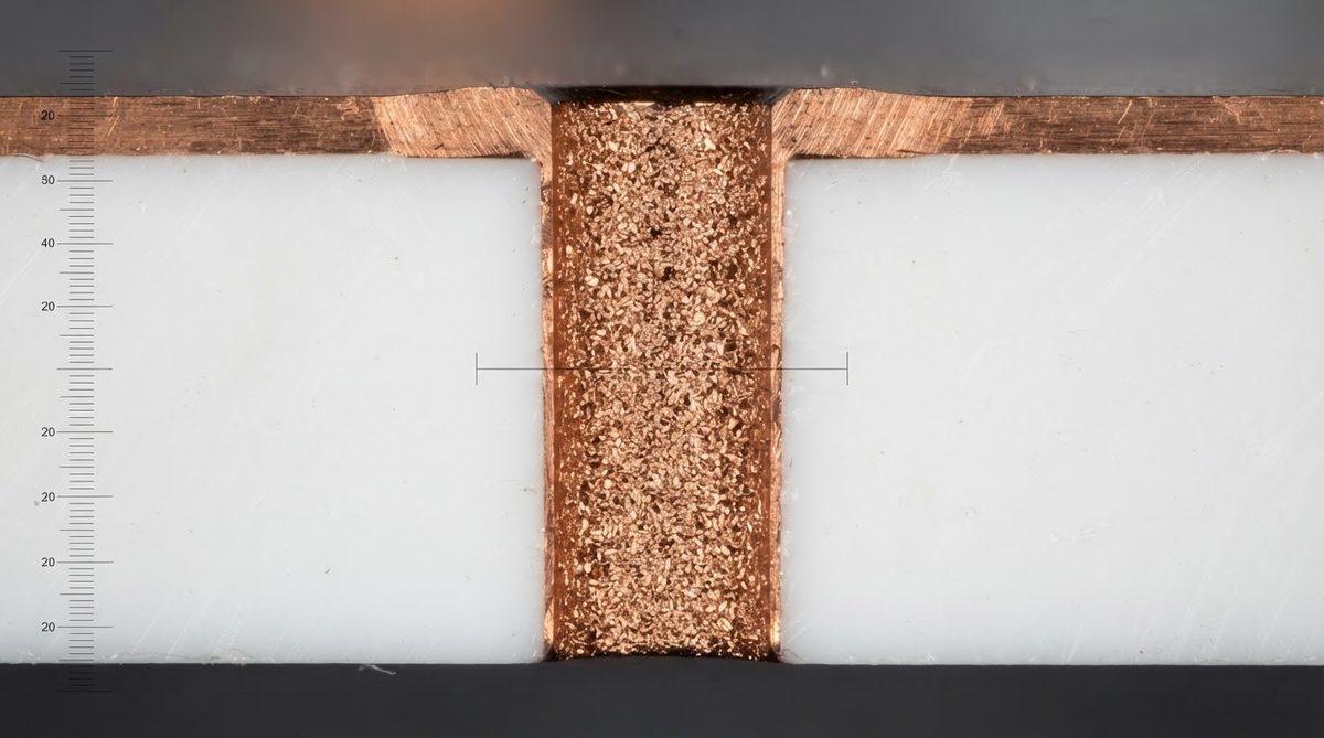
Bare ceramic is non-conductive and chemically inert. You cannot plate copper directly onto Al₂O₃ or AlN the way you would onto an FR-4 laminate with exposed glass fibers. A metallization seed layer must be deposited first. The two dominant approaches are sputtering (PVD) and electroless activation.
In the DPC (Direct Plated Copper) process, a thin adhesion layer of titanium or chromium (50–200 nm) is sputtered onto the ceramic, followed by a copper seed of 200–500 nm. Electrolytic copper is then built up to the target thickness through pattern plating or panel plating. This sequence gives the tightest line/space resolution available on ceramic boards and defines the upper range of copper plating ceramic capability for fine-pitch designs.
For thick-film metallized substrates, copper paste is screen-printed and fired first, then electroplated to increase thickness or improve surface conductivity. The fired thick-film layer acts as the seed, but its surface roughness (Ra 1–3 µm) is higher than a sputtered seed, which affects fine-line capability.
Copper Plating Thickness Ranges and Tolerances
| Parameter | Electroless Seed | Electrolytic (Pattern) | Electrolytic (Panel) |
|---|---|---|---|
| Thickness range | 0.3–1.5 µm | 5–70 µm | 10–300 µm |
| Thickness tolerance | ±20 % | ±10 % | ±10 % |
| Current density | N/A (chemical) | 1–3 A/dm² | 2–4 A/dm² |
| Typical bath | Alkaline Cu | Acid Cu sulfate | Acid Cu sulfate |
| Min line/space achievable | N/A (blanket) | 30/30 µm | 75/75 µm (post-etch) |
| Surface roughness (Ra) | 0.2–0.5 µm | 0.3–0.8 µm | 0.5–1.2 µm |
Typical values for commercially available processes, for comparison only. Confirm against the datasheet for your specific grade and plating vendor.
Pattern plating deposits copper only inside photoresist openings, so the plated area is smaller and current distribution is more uniform. This is why DPC lines can hold 30/30 µm trace/space. Panel plating covers the entire surface and is then etched back, which limits practical resolution to about 75/75 µm due to etch undercut.
Worked Example: Plating Thickness for a 20 A Power Trace
Suppose you need a 3 mm wide trace to carry 20 A continuous on an Al₂O₃ 96 % substrate with a maximum temperature rise of 30 °C. Using the simplified IPC-2152 cross-section method for external traces:
- Required cross-section area ≈ 0.065 mm² (from IPC-2152 charts at 20 A, 30 °C rise, external layer).
- Cross-section = width × thickness → 0.065 mm² / 3 mm = 0.0217 mm = 21.7 µm minimum copper thickness.
- Add 10 % tolerance margin → target plating thickness = 24 µm.
- This sits comfortably within the 5–70 µm pattern-plating window. No need to move to thick copper processes.
If the same trace needed 50 A, the required thickness jumps to roughly 90 µm at 3 mm width, pushing you into panel plating or a DBC approach. Knowing the full copper plating ceramic capability range up front prevents costly process changes mid-project.
Enter your trace width, target current, and allowable temperature rise below to check whether standard plating thickness covers your design.
Adhesion and Peel Strength
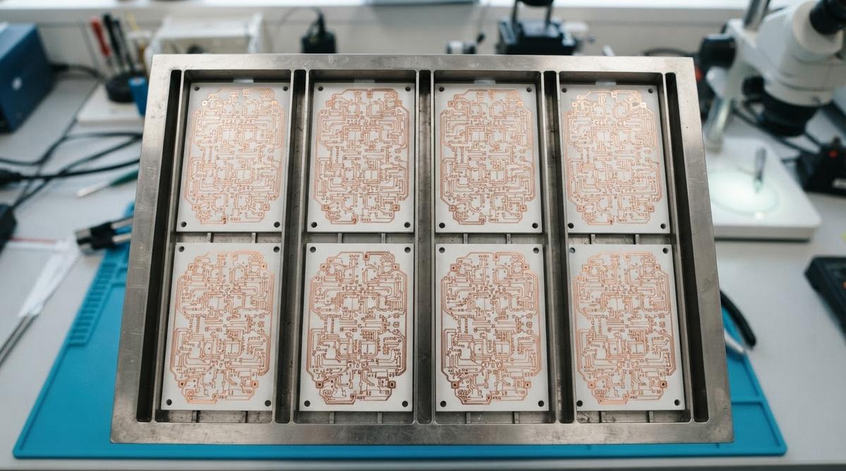
Adhesion is the failure mode that separates ceramic plating from FR-4 plating. On organic laminates, copper bonds mechanically to roughened glass-epoxy. On ceramic, adhesion depends entirely on the seed-layer metallurgy.
A Ti/Cu sputtered seed on polished Al₂O₃ 96 % typically yields 6–10 N/cm peel strength (90° peel test, per IPC-TM-650 2.4.8). A Cr/Cu seed on AlN is slightly lower, 5–8 N/cm, because AlN’s surface oxidizes rapidly and the Cr–AlN interface is sensitive to moisture. For comparison, DBC (Direct Bonded Copper) achieves 8–14 N/cm because the Cu–Al₂O₃ eutectic bond is thicker and more mechanically interlocked.
Thermal cycling degrades plated adhesion faster than DBC adhesion. After 1,000 cycles from −40 °C to +150 °C, sputtered-seed plated copper typically retains 70–85 % of its initial peel strength, while DBC retains 90 %+ (per CeramTec reliability data). If your application requires deep thermal cycling, factor this degradation into your design margin.
Via Fill Plating on Ceramic
Plating copper into laser-drilled vias on ceramic follows the same electrochemistry as on organic boards, but the via geometry is different. Ceramic vias are typically straighter-walled (nearly vertical) because laser drilling on ceramic produces less taper than on resin-glass laminates.
For aspect ratios below 3:1, DC plating with standard brightener/leveler chemistry fills vias reliably. Above 3:1, pulse-reverse plating is necessary to avoid center voids. A common waveform is 10 ms forward at 3 A/dm², 2 ms reverse at 1.5 A/dm². Via filling tolerances on ceramic typically allow a dimple depth of ≤15 µm post-planarization. This aspect of copper plating ceramic capability is often the gating factor in multilayer ceramic circuit designs.
When Copper Plating Is Not the Right Choice
Plating is not always the best metallization path for ceramic. Consider alternatives in these situations:
- Copper thickness above 300 µm. DBC or AMB bonds pre-formed copper foil and handles 300–800 µm without the stress and bath-time issues of heavy plating.
- Budget-constrained prototypes with ≥100 µm lines. Thick-film screen printing followed by a single flash plate is faster and cheaper than full DPC sputtering plus pattern plating.
- High-frequency RF circuits needing Ra below 0.2 µm. Thin-film sputtering with no plating step produces smoother copper. See thin-film copper capabilities for details.
- Applications on FR-4 or metal-core PCBs. If your operating temperature stays below 130 °C and thermal conductivity above 1 W/mK is sufficient, ceramic adds cost without proportional benefit.
FAQ
Can you plate copper directly onto raw ceramic without a seed layer?
No. Ceramic is electrically insulating and chemically inert, so electrolytic copper will not deposit on it. An adhesion/seed layer (sputtered Ti/Cu, Cr/Cu, or electroless Pd/Cu activation) must be applied first. Skipping this step results in zero adhesion.
Does copper plating on ceramic pass MIL-STD-883 adhesion testing?
Yes, when the seed layer is properly deposited. Sputtered Ti/Cu on Al₂O₃ 96 % routinely passes the MIL-STD-883 Method 2019 die shear and peel tests. AlN substrates require tighter process control on the sputtering atmosphere to pass consistently.
How does plating uniformity compare between ceramic and FR-4?
Ceramic panels are flatter and more dimensionally stable than FR-4, so plating uniformity is often better—±10 % on ceramic versus ±15–20 % on thin FR-4 panels that flex in the plating fixture. The main risk on ceramic is edge-to-center thickness variation on large panels.
What surface finishes can be applied over plated copper on ceramic?
All standard PCB finishes work: ENIG, ENEPIG, immersion silver, immersion tin, OSP, and electrolytic gold or nickel-gold. The choice depends on solderability, wire-bondability, and shelf-life requirements, not on the ceramic substrate itself.
Is copper plating on ceramic RoHS-compliant?
Yes. Acid copper sulfate baths are lead-free. The seed-layer metals (Ti, Cr, Cu) and the plated copper contain no restricted substances under RoHS Directive 2011/65/EU. Confirm that any brightener or leveler additives in the bath are also compliant with your supply-chain requirements.