A coplanar waveguide ceramic substrate holds controlled impedance from DC to beyond 110 GHz because ceramics offer dielectric-constant tolerances of ±1–2 %, loss tangents below 0.001 at 10 GHz, and surface roughness under 0.4 µm on polished grades. That combination is difficult or impossible to achieve on organic laminates, which is why nearly every mmWave test fixture, MMIC carrier, and satellite feed network builds its coplanar waveguide ceramic transmission lines on alumina or aluminum nitride.
What Is a Coplanar Waveguide on Ceramic?
A coplanar waveguide (CPW) is a planar transmission line where the signal conductor and both ground planes sit on the same surface of a dielectric substrate. The characteristic impedance is set by the ratio of the center-strip width (W) to the gap (G) between signal and ground, along with the substrate’s dielectric constant (εr) and thickness (h). Because all conductors are on one side, CPW eliminates vias to ground, simplifies flip-chip and wire-bond attachment, and gives easy access for on-wafer probing.
Two common variants exist. Grounded CPW (GCPW or CBCPW) adds a ground plane on the backside, which suppresses parallel-plate modes and improves isolation at the cost of requiring backside metallization and ground vias. Ungrounded CPW uses no backside metal, keeping fabrication simple but limiting usable bandwidth before substrate modes appear.
Why Ceramic for Coplanar Waveguide Designs?
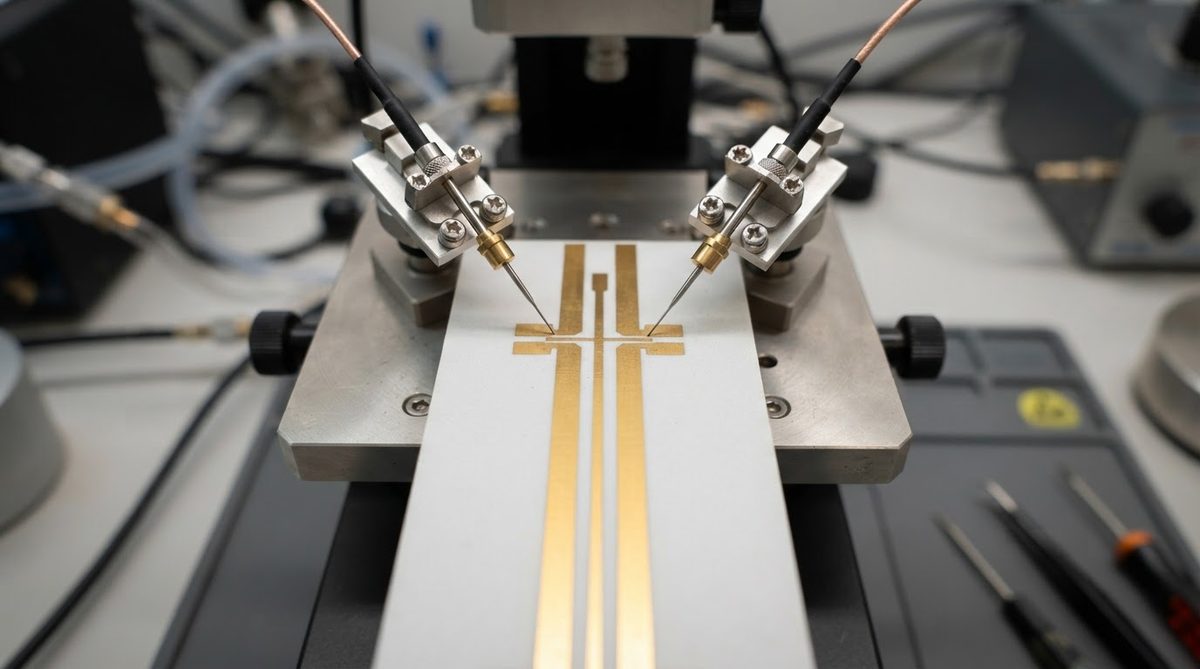
Three properties make coplanar waveguide ceramic substrates dominant in CPW applications above 10 GHz.
- Tight εr tolerance. 96 % alumina holds εr = 9.6 ± 0.2 at 10 GHz (per CoorsTek ADS-96R datasheet). A ±2 % swing in εr shifts 50 Ω impedance by roughly ±1 Ω. On FR-4 (εr tolerance ±5–10 %), the same shift can reach ±3–5 Ω.
- Low dielectric loss. Alumina’s tan δ of 0.0001–0.0004 at 10 GHz keeps conductor loss dominant, so your loss budget stays predictable. See the full comparison of ceramic substrate loss tangent at RF and mmWave frequencies.
- Dimensional stability. Ceramic does not absorb moisture, swell, or shift CTE with humidity. Line widths fired or laser-cut to ±5 µm stay there over temperature and time.
Coplanar Waveguide Ceramic Material Selection
| Parameter | Al₂O₃ 96 % | Al₂O₃ 99.6 % | AlN | Unit | Condition | Source |
|---|---|---|---|---|---|---|
| εr | 9.6 | 9.9 | 8.6 | — | 10 GHz, 25 °C | CoorsTek / Kyocera datasheets |
| tan δ | 0.0002–0.0004 | 0.0001–0.0002 | 0.0003–0.001 | — | 10 GHz, 25 °C | CoorsTek / Maruwa datasheets |
| Thermal conductivity | 24–28 | 30–35 | 170–200 | W/mK | 25 °C | Kyocera / CoorsTek |
| Surface roughness (Ra, polished) | 0.1–0.4 | 0.05–0.15 | 0.2–0.5 | µm | Polished face | Maruwa SPC series |
| CTE | 7.2 | 7.1 | 4.5 | ppm/°C | 25–300 °C | CoorsTek |
Typical values for commercially available material, for comparison only. Confirm against the datasheet for your specific grade.
For most coplanar waveguide ceramic work below 40 GHz, 96 % alumina is the cost-effective default. Move to 99.6 % alumina when you need lower surface roughness for reduced conductor loss above 60 GHz. Choose AlN only when thermal dissipation is the binding constraint—for example, a GaN PA carrier where the die must stay below 150 °C. The ceramic substrate thickness chart helps you pick a standard thickness that supports your target impedance without custom lapping.
CPW Geometry and Impedance: Worked Example
The characteristic impedance of a CPW on an infinitely thick substrate is approximated by:
Z₀ = (30π / √εeff) · K(k’) / K(k)
where k = W / (W + 2G), k’ = √(1 − k²), and K is the complete elliptic integral of the first kind. εeff ≈ (εr + 1) / 2 for ungrounded CPW on a substrate much thicker than the gap.
Example: 50 Ω CPW on 0.635 mm, 96 % Alumina
Target: Z₀ = 50 Ω, εr = 9.6, substrate thickness h = 0.635 mm.
- εeff ≈ (9.6 + 1) / 2 = 5.3 (first-order; full-wave simulation refines this to ~5.1 for finite h).
- For Z₀ = 50 Ω, K(k’)/K(k) ≈ 50 · √5.3 / (30π) ≈ 1.22.
- From elliptic integral tables, k ≈ 0.44, so W / (W + 2G) = 0.44.
- Pick W = 100 µm → 2G = 127.3 µm → G ≈ 64 µm each side.
- Check: h / (W + 2G) = 635 / 227.3 ≈ 2.8. Because h > 2 × (W + 2G), the infinite-substrate approximation is reasonable. For thinner substrates or GCPW, use a 2.5-D field solver.
This geometry is well within the capability of thin-film or DPC metallization. If your process uses thick-film screen printing, minimum gap is typically 75–100 µm, which pushes W wider. Verify your fabricator’s copper plating tolerances before finalizing trace and gap dimensions.
Use the calculator below to sweep signal width, gap, and substrate parameters for microstrip or quasi-CPW impedance on alumina and other ceramic substrates.
[pcb_calc type=”microstrip-impedance”]
Loss Budget: Where Do the dB Go?
Total CPW loss has three components: conductor loss (αc), dielectric loss (αd), and radiation loss (αr). On a coplanar waveguide ceramic substrate, dielectric loss is almost negligible, so the design fight is against conductor loss and radiation.
Conductor Loss
At 30 GHz on 96 % alumina with 3 µm gold metallization (ρ = 2.44 µΩ·cm), a 50 Ω CPW with W = 100 µm and G = 64 µm shows αc ≈ 0.15–0.20 dB/mm (per Ponchak & Downey, NASA/TM-2002-211661). Surface roughness matters: a polished 99.6 % alumina substrate (Ra 0.1 µm) cuts conductor loss by 10–15 % versus as-fired 96 % (Ra 0.3–0.5 µm) at the same frequency, because the skin depth at 30 GHz is only ~0.45 µm in gold.
Dielectric Loss
αd = (π · f · √εeff · tan δ) / c. At 30 GHz with εeff = 5.1 and tan δ = 0.0003: αd ≈ 0.021 dB/mm. This is roughly one-tenth of conductor loss, confirming that metallization quality and surface finish dominate the loss picture in any coplanar waveguide ceramic design.
Radiation Loss
Radiation loss rises sharply when substrate thickness exceeds λg/10. At 60 GHz on εr = 9.6, λg ≈ 1.6 mm, so keep h ≤ 0.16 mm—use a 0.127 mm or 0.15 mm substrate. A backside ground (GCPW) suppresses substrate modes and relaxes this limit somewhat.
Grounded vs. Ungrounded CPW on Ceramic
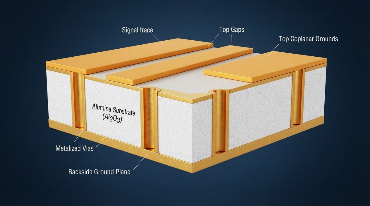
| Parameter | Ungrounded CPW | Grounded CPW (GCPW) |
|---|---|---|
| Backside metallization | None | Full ground plane |
| Ground vias required | No | Yes, spaced ≤ λ/20 |
| Substrate-mode suppression | Poor above ~40 GHz on 0.635 mm | Good to 110 GHz on 0.127 mm |
| Fabrication complexity | Single-side metallization | Double-side + via drilling/filling |
| Flip-chip compatibility | Excellent | Excellent |
| Typical use | Probe calibration standards, simple interconnects | MMIC carriers, phased-array feeds, satellite filters |
For most production RF boards, GCPW is the safer choice. The added cost of backside metallization and laser-drilled vias is small compared to the risk of spurious modes corrupting your S-parameters at high frequency.
Practical Design Rules for Coplanar Waveguide Ceramic Circuits
- Ground-plane width. Each coplanar ground strip should be at least 3 × (W + 2G) wide, or tied to the backside ground with vias, to avoid ground-inductance problems.
- Via spacing for GCPW. Place ground vias at intervals ≤ λg/20 at your highest operating frequency. At 77 GHz on alumina, that is roughly 0.1 mm pitch—achievable with laser drilling.
- Transitions. CPW-to-microstrip transitions are common when routing to connectors. A tapered ground with via stitching over 0.3–0.5 λg keeps return loss below −20 dB. The microstrip width calculator for alumina helps size the microstrip section of the transition.
- Wire-bond compensation. A 25 µm gold wire bond adds ~0.3–0.5 nH. Compensate with a short high-impedance section (narrower W) immediately before the bond pad.
When Not to Use Ceramic CPW
Ceramic CPW is overkill—and over-budget—in several common situations.
- Below 6 GHz with relaxed loss specs. Rogers RO4003C or Isola Astra MT77 on standard PCB processes will hold 50 Ω adequately and cost a fraction of ceramic.
- Large-area boards (> 100 × 100 mm). Ceramic substrates rarely exceed 150 × 150 mm, and warpage and cost both rise fast. Use PTFE-ceramic laminates instead.
- High-layer-count digital-RF integration. If you need 8+ layers with embedded passives and high-speed digital, LTCC or organic HDI is a better architecture than single-layer ceramic CPW.
- Cost-sensitive consumer products. Ceramic substrates start at roughly 5–15× the cost of FR-4 per unit area. If your BOM cannot absorb that, ceramic is the wrong substrate.
Frequently Asked Questions
Can I use screen-printed thick-film metallization for CPW above 40 GHz?
Thick-film silver or gold paste typically achieves minimum line/space of 75–100 µm and surface roughness of 1–3 µm. Above 40 GHz, where skin depth drops below 0.5 µm, that roughness adds significant conductor loss. Thin-film sputtered gold or copper with photolithographic patterning is the standard choice for frequencies above 30–40 GHz.
Does substrate thickness affect CPW impedance?
Yes. When the substrate is thinner than roughly 2 × (W + 2G), the backside boundary (air or ground plane) shifts εeff and changes Z₀. For GCPW on a 0.127 mm substrate with W = 50 µm and G = 30 µm, the impedance can drop 3–5 Ω compared to the infinite-substrate approximation. Always use a field solver for thin substrates.
What surface finish works best for ceramic CPW?
Sputtered gold (0.5–3 µm) over a Ti/TiW adhesion layer is the most common finish for wire-bondable CPW. For solder-attach applications, electroless nickel / immersion gold (ENIG) works, but the nickel layer’s ferromagnetic loss can degrade performance above 20 GHz. Specify non-magnetic nickel (phosphorus content > 10 %) or skip nickel entirely if loss is critical.
How do I transition from CPW to a coaxial connector?
The standard approach is a CPW-to-microstrip taper followed by a microstrip-to-coax launcher (e.g., Southwest Microwave end-launch). The taper length should be 0.3–0.5 guided wavelengths, with via stitching along both ground edges. Alternatively, vertical coax-to-CPW launchers from Anritsu or Rosenberger probe directly onto the CPW pads for test fixtures.
Is AlN better than alumina for coplanar waveguide ceramic applications?
AlN’s lower εr (8.6 vs. 9.6) gives slightly wider traces for 50 Ω, easing fabrication tolerances. Its higher thermal conductivity (170–200 W/mK) helps when the CPW carries power, such as in a GaN PA output network. However, AlN costs 3–5× more than 96 % alumina and has a slightly higher tan δ at 10 GHz. For passive interconnects and filters, alumina is the better value.
Next Step
If you are designing a coplanar waveguide on ceramic, start by selecting a blank ceramic substrate in the thickness and grade your impedance model requires. For thermal management under active devices on the same substrate, review ceramic heat spreader design guidelines. When your layout is ready, request a quote to confirm line/space capability and lead time for your specific geometry.