These thick film ceramic layout guidelines are driven by the screen-printing process: a mesh screen pushes conductive paste onto the substrate, then the assembly is fired at 850–1000 °C. Every dimension you draw must account for paste spread, mesh resolution, and shrinkage during firing. Following proven thick film ceramic layout guidelines from the start means your first prototype does not become an expensive learning exercise. The concrete numbers below cover traces, vias, pads, tolerances, and panel breakout.
Key Takeaways
- Minimum trace width for standard thick-film screen printing is 100–125 µm (4–5 mil); minimum space is the same.
- Fired conductor thickness typically ranges from 8–15 µm per print pass, with tighter sheet-resistance control at 10–12 µm.
- Via diameters should be ≥ 200 µm (8 mil) for reliable paste fill; smaller vias risk incomplete filling and voids.
- Pad-to-edge clearance of ≥ 300 µm (12 mil) prevents cracking during laser scribing or snap-line breakout.
- Design for ± 25 µm positional tolerance on all printed features relative to substrate edges and vias.
Minimum Trace Width and Spacing in Thick Film Ceramic Layout Guidelines
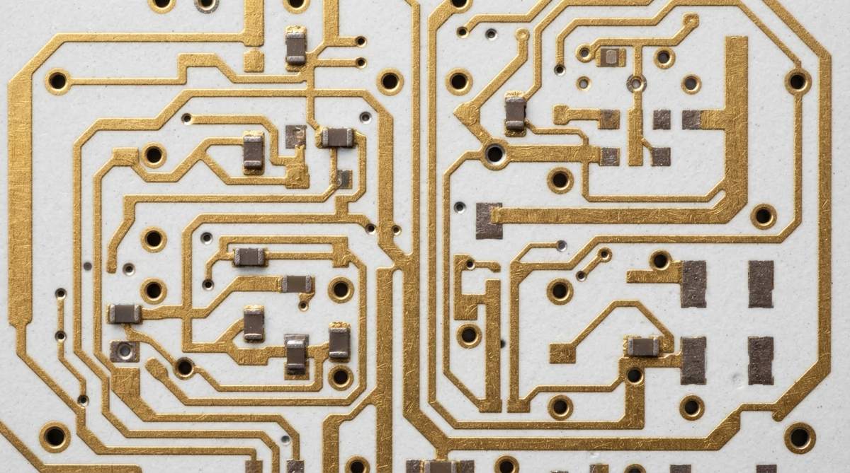
Standard thick-film screen printing on 96% alumina substrates uses a 325- or 400-mesh stainless steel screen. This limits the practical minimum line width to about 100–125 µm. Finer meshes (500-mesh) can push this toward 75 µm, but yield drops and paste rheology becomes critical. Unless your design absolutely requires sub-100 µm features, stay at 125 µm or wider.
Minimum space between conductors follows the same floor: 100–125 µm. Below that, paste bridging between adjacent traces rises sharply. For power circuits where creepage matters, consult IEC 60664-1 for the required clearance at your working voltage; the process minimum is rarely the limiting factor on high-voltage ceramic boards.
If your circuit demands finer features—50 µm lines or below—you need a photolithographic process, not screen printing. See the thin film ceramic layout rules for those design constraints.
Conductor Thickness and Sheet Resistance
A single screen-print pass deposits 8–15 µm of fired conductor, depending on paste viscosity, screen emulsion thickness, and squeegee pressure. Two passes can reach 20–25 µm. Gold, silver, and silver-palladium pastes each have different fired densities, so sheet resistance varies:
| Paste type | Fired thickness (µm) | Sheet resistance (mΩ/□) | Condition |
|---|---|---|---|
| Ag (silver) | 10–12 | 1.5–3.0 | Fired 850 °C, single pass |
| AgPd (silver-palladium) | 10–12 | 20–80 | Fired 850 °C, Pd content dependent |
| Au (gold) | 8–10 | 3–5 | Fired 850 °C, single pass |
| RuO₂ resistor | 10–15 | 10 Ω/□ – 1 MΩ/□ | Composition dependent |
Typical values for commercially available pastes from DuPont, Heraeus, and ESL. Confirm against the datasheet for your specific grade.
For low-loss RF or high-current paths, thick-film silver metallized ceramic gives the lowest resistivity per print. If you need even lower resistance, a post-fire copper plating step can add bulk conductivity; see copper plating capabilities and tolerances for thickness options.
Pad Geometry and Component Attach
Pad dimensions must account for paste spread after printing (typically 15–25 µm per edge) and positional tolerance of ± 25 µm. A practical rule within these thick film ceramic layout guidelines: make each pad at least 50 µm larger per side than the nominal land pattern you would use on an FR-4 board.
For wire-bond pads, keep the bonding area at least 200 × 200 µm for gold ball bonding and 300 × 300 µm for aluminum wedge bonding. Surface roughness of fired thick-film gold is typically Ra 0.3–0.8 µm, which is acceptable for both bond types without polishing.
For solder-attach pads (die attach or SMD), ensure the pad extends at least 150 µm beyond the component footprint on each side. This extra margin lets solder fillets form and provides visual inspection access.
Via Design and Placement
Thick-film vias are punched or laser-drilled in the green (unfired) substrate, then filled with conductive paste and co-fired. The minimum reliable via diameter is 200 µm (8 mil). Smaller vias can be drilled, but paste fill becomes inconsistent and void rates climb above 10%.
Place vias at least 300 µm (center-to-center) from any substrate edge or snap line. Closer placement risks micro-cracks propagating from the breakout line into the via barrel. For dense via arrays, maintain a center-to-center pitch of ≥ 2× the via diameter to preserve substrate integrity between holes.
If your design needs filled and capped vias for thermal or electrical continuity, review the ceramic via filling process to understand fill materials and inspection criteria.
Worked Example: Via Pitch on a Power Hybrid
Suppose you need 12 thermal vias under a 3 × 3 mm die-attach pad, each via 250 µm diameter. Minimum pitch = 2 × 250 µm = 500 µm center-to-center. In a 3 mm span you can fit 3 mm / 0.5 mm = 6 vias per row. A 6 × 2 array gives 12 vias, occupying a 2.5 mm × 0.5 mm footprint—well within the pad area.
Enter your via diameter, count, and pad area below to check whether your thermal via array fits within your die-attach footprint and meets the spacing rules from these thick film ceramic layout guidelines.
Substrate Panel and Breakout Considerations
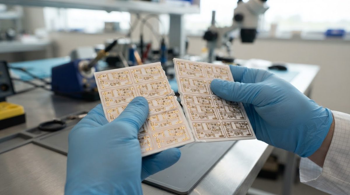
Thick-film circuits are usually printed on a larger panel, then singulated by laser scribing and snap-breaking. The scribe line weakens the ceramic along a controlled path, so your layout must respect a keep-out zone of ≥ 300 µm on each side of the scribe line. No conductors, resistors, or vias should fall inside this zone.
Panel utilisation matters for cost. Work with standard substrate blanks—commonly 114.3 × 114.3 mm (4.5″ × 4.5″) for 96% alumina. If your individual circuit is 25 × 25 mm, a 4 × 4 array with 0.3 mm scribe streets yields 16 units per panel. Adding fiducials and test coupons at the panel border costs you one row but improves registration and quality data.
Registration and Tolerance Stack
Each print pass introduces its own alignment error. Typical layer-to-layer registration on a well-maintained thick-film line is ± 25–50 µm. If your design has three print layers (conductor, resistor, dielectric), the worst-case stack is 3 × 50 µm = 150 µm. Design overlaps (e.g., resistor termination overlap onto conductor pads) accordingly—a minimum 150 µm overlap is standard practice.
Substrate dimensional tolerance after firing is ± 1% of the linear dimension per ASTM C1161. For a 25 mm part, that is ± 250 µm. Mechanical mounting features—slots, tooling holes—should allow for this. Applying these thick film ceramic layout guidelines to your tolerance stack early prevents costly re-spins later.
When Thick Film Is Not the Right Choice
Thick film is the workhorse for hybrid circuits, power modules, and sensors. But it has limits. Choose a different process if:
- Trace/space below 75 µm: You need thin-film photolithography. Review design rules for thin film ceramic PCBs instead.
- High-frequency impedance-controlled lines above 20 GHz: Thick-film conductor edges are too rough (± 15–25 µm) for tight impedance control. Thin film on 99.6% alumina or AlN is the standard approach at these frequencies.
- Conductor thickness above 30 µm without plating: Multiple print passes degrade definition. DBC or plated copper is more practical for bulk current carrying.
- Standard digital logic with hundreds of nets: FR-4 or LTCC multilayer is cheaper and faster. Ceramic thick film makes sense when thermal, high-voltage, or harsh-environment requirements rule out organic boards.
Frequently Asked Questions
What is the tightest trace/space achievable with thick film?
About 75 µm (3 mil) with a fine 500-mesh screen on a flat, well-prepared substrate. Production yields are significantly better at 100–125 µm, so most manufacturers quote that as the standard minimum.
Can I print thick-film conductors on aluminum nitride?
Yes. AlN-compatible pastes (typically gold- or silver-based with modified glass frits) are available from Heraeus and DuPont. The same thick film ceramic layout guidelines apply, but firing profiles differ. See the AlN thick film substrate page for material-specific details.
How do I handle crossover routing on a single-layer thick-film circuit?
Print a dielectric pad over the lower conductor, fire it, then print the crossover conductor on top. The dielectric patch should extend at least 200 µm beyond the lower trace on each side to prevent arcing. Keep crossovers to a minimum—each one adds a print-and-fire cycle.
Do I need to derate trace width for high current on thick film?
Yes. A 250 µm wide, 12 µm thick silver trace can carry roughly 1–1.5 A continuously in still air on alumina, based on a 20 °C temperature rise. For higher currents, widen the trace or add a plated copper overlay. There is no IPC-2152 equivalent for ceramic thick film; use the paste manufacturer’s current-capacity data or run a thermal simulation.
What file format should I submit for thick-film artwork?
Gerber RS-274X is the standard. Supply one layer file per print pass (conductor, resistor, dielectric, solder mask if used) plus a drill file for vias and an outline layer showing scribe lines. Include a fabrication drawing with tolerances, paste callouts, and firing sequence notes.
Is thick-film ceramic suitable for flex or curved surfaces?
No. Ceramic substrates are rigid and brittle. Thick-film paste cannot be printed on a curved surface. If you need a conformal circuit, look at flex-PCB or printed electronics on polyimide.